
In this post, we’ll show you exactly how to unlock the power of Flux Copilot for yourself: from writing rock-solid triggers to scoping entries at the project, user, and system levels.
If you're looking to improve your understanding of schematic diagrams, this article is the perfect starting point. Let's explore the crucial role of circuits and components schematics in translating conceptual electrical designs into physical printed circuit board assemblies (PCBAs).
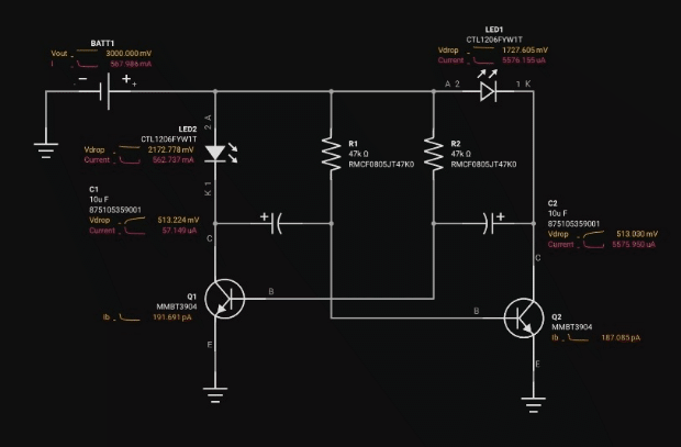
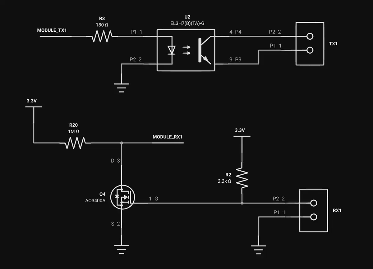
A schematic diagram, or schematic drawing, is a fundamental two-dimensional circuit representation showing the functionality and connectivity between different electrical components. It's composed of electronic symbols, wiring diagrams, designators, net names, and netlist. A PCB designer needs to get familiarized with the schematic symbols that represent the components on a schematic diagram. These symbols serve as a universal language understood by engineers, technicians, and electricians across different industries. They provide a concise and standardized way of communicating circuit designs.
A schematic block diagram also referred to as a block diagram or a functional diagram, is a simplified representation of a system or a process using blocks to represent its various components or stages. It provides an overview of the system's structure and the interconnections between its major functional units or subsystems.
In a schematic block diagram, each block represents a specific component, module, or function within the system. The blocks are typically labeled with descriptive text to indicate their purpose or functionality. The interconnections between the blocks are represented by lines or arrows, indicating the flow of signals, information, or energy between the different components or stages.
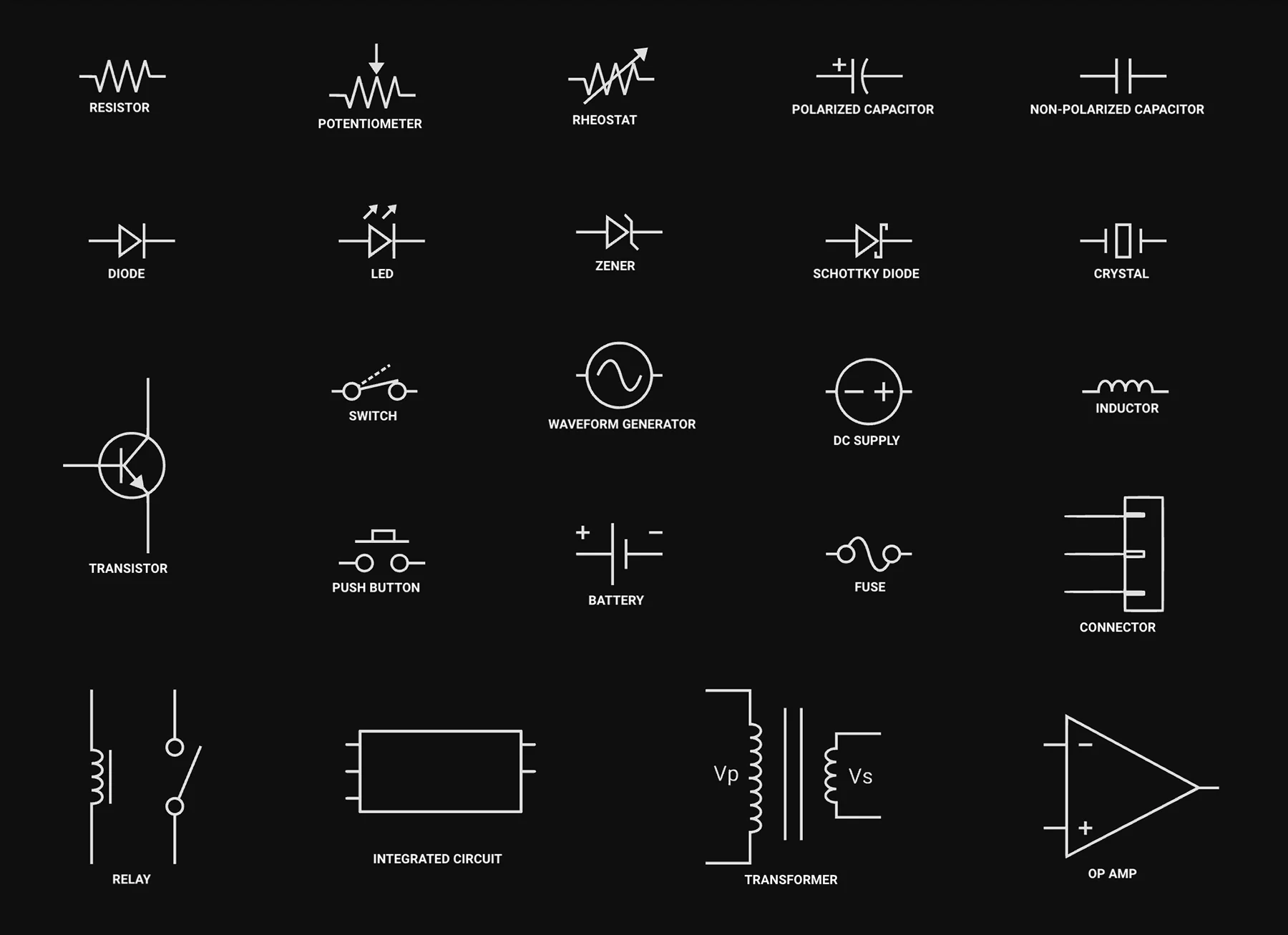
Schematic symbols are typically designed to visually represent the physical characteristics, electrical properties, and functionality of components. They are usually simple, abstract, and intuitive, allowing quick recognition and identification.
For example, a resistor in a circuit diagram is represented by a zigzag line, which indicates its function of restricting current flow. A capacitor is depicted by two parallel lines separated by a gap, representing its ability to store electrical energy. Symbols exist for diodes, transistors, switches, connectors, IC (integrated circuits), and many other components used in electrical circuits and electronic circuits.
Each component in a schematic diagram is assigned a component designator or reference designator (REFDES) to indicate its specific function within the circuit. It is a letter or combination of letters used to identify individual components within a circuit diagram uniquely. The designators serve as labels or identifiers for the components and are typically placed next to the corresponding symbols in the circuit diagram. It is important to follow a consistent and well-defined designator system within a circuit diagram to ensure clear communication and easy referencing of components.
Reference designators play a crucial role in the connection to the bill of materials (BOM). The BOM contains the part number for each component in your PCBA design and specifies where each part should be installed, based on its reference designator (REFDES).
Here are industry-standard formats for reference designators including a letter, indicating the type of component, followed by a number. For example R1, R2, R3.. etc
IEC 60617 and ANSI standard Y32 are two widely recognized and used standards for schematic diagram symbols and graphical representations in electrical and electronic circuit diagrams. These standards provide guidelines for the consistent depiction of components, connections, and other elements in circuit diagrams, ensuring clear communication and interoperability.
Both standards cover a wide range of components, including passive elements (resistors, capacitors, inductors), active devices (transistors, diodes), power sources, switches, connectors, logic gates, and more. They are periodically updated to incorporate new symbols, reflect technological advancements, and address industry needs.
The schematic diagram should provide this additional information to ensure that appropriate components are selected. The resistor should have its resistance value expressed in ohms (Ω). The battery should state its potential difference (voltage) expressed in volts. Other components are described in different terms. For example, capacitors differ by their capacitance value expressed in farads (F), and inductors are differentiated by their inductance value expressed in Henrys (H).
Additional attributions can be given to the symbols like power ratings, values, tolerances, etc. This helps us in identifying the correct components for the circuit. Here are common attributes of a component are:
Explore the key aspects of PCB thermal analysis and discover best practices for enhancing your PCB design. Understand how thermal conductivity impacts heat management and overall PCB functionality, leading to more reliable and efficient circuits.
Electric currents generate heat as they pass through resistive elements of a circuit. The higher the resistance of a conductor, the more heat will be generated as current passes through it. Therefore, addressing both electric and thermal parameters in board design is essential for long-term functionality. PCB thermal analysis plays a vital role in the design process, as it can predict thermal flaws and provide an opportunity for circuit redesign. Some key PCB design considerations for improved thermal performance include temperature-sensitive components. Components that are especially sensitive to temperature should be placed in the location with the lowest temperature, such as the bottom of the board.
The simplest way to dissipate heat would be through thermal vias to the cooling system (heat sink or heat pipes). The heat sink draws heat away from the PCB to fins that provide a larger surface area for faster heat dissipation.
Thermal Equivalent Circuits are an analogy of electrical circuits to provide an estimation of the flow of heat in a design. They work because the underlying equations for the transfer of thermal energy and electrical energy are similar enough. With the analogies, we can calculate the heat transfer within the PCB.
Equivalent Equations
I = V1-V2/R => Q = T1-T2/Rt
Where:
I is the current (A)
V is the voltage (V)
R is the electrical resistance
Q is the heat flow (W)
T is the junction temperature (°C)
Rt is the thermal resistance (°C/W)
Similarly, equivalent thermal resistance in series and parallel also follows the same equations for electrical resistance.
Thermal impedance measures the sum of thermal resistance and thermal contact resistance of a material. This value can be found in the component datasheet for integrated circuits and ranges from 20 °C/W for low-power amplifiers or ICs, to as high as ~200 °C/W for powerful microprocessors. The operating temperature can be determined by multiplying the component’s power consumption by its thermal impedance.
T = Z*P
Where:
T is the component temperature (°C).
P is the power usage of the component (W)
Z is the thermal impedance (°C/W)
When your PCB generates significant heat, choosing a substrate with superior thermal conductivity is crucial. Ceramics are an excellent option due to their high thermal conductivity and adjustable mechanical properties, which help manage mechanical stress during thermal cycling. Adding a metal core to the board or increasing copper below components, such as adding a plane layer, can also enhance heat dissipation.
When designing PCBs, the importance of effective thermal management cannot be overstated. High-power components generate significant heat, and without proper dissipation, the performance and longevity of the circuit boards can be compromised. One effective method to manage this heat is by using a heat sink. A heat sink helps to draw heat away from critical components, improving the overall thermal performance of the PCB.
Thermal relief is also design feature used in electronic circuit boards to manage heat dissipation from components that generate significant heat during operation. It helps to prevent overheating and ensures the reliability and longevity of the components.

There are two main configurations for thermal relief:
PCBs are the backbone of modern electronics, and ensuring they operate within safe thermal limits is crucial. Circuit boards that overheat can lead to component failure and reduced reliability. This is why thermal resistance and thermal impedance are important parameters to consider in PCB design. By carefully selecting materials and employing efficient cooling techniques, such as integrating cooling fans, the thermal performance of PCBs can be significantly enhanced.
PCB thermal simulation enables designers to predict thermal management issues, ensuring optimal heat dissipation. By simulating different layouts and thermal solutions, designers can avoid costly physical iterations and achieve a thermally efficient design from the outset.
Thermally conductive materials, such as certain ceramics, can greatly improve the heat dissipation capabilities of circuit boards. Additionally, incorporating thermal vias and using thermally conductive paste can further aid in managing the heat generated by high-power components. Cooling fans are another essential element in thermal management, ensuring that heat is effectively removed from the PCB and dissipated into the surrounding environment.
PCB design requires careful consideration of thermal management techniques. By utilizing heat sinks, thermally conductive materials, and cooling fans, designers can create circuit boards that operate efficiently and reliably, even under demanding conditions. Proper thermal analysis and simulation are key to achieving optimal performance and preventing overheating issues in PCBs.

Let’s start by exploring the benefits of SMDs, as opposed to traditional through-holes:
Surface Mount Device (SMD) packaging for passive components, such as resistors, capacitors, and inductors, involves a variety of package types:
SMDs come with their own set of challenges during assembly and use:

This blog post explores the RS485 communication standard, renowned for its ability to facilitate long-distance, multidrop networking with enhanced noise immunity, making it a preferred choice for industrial settings. Dive into the post to understand RS485's key features and advantages over older protocols.
RS485 is engineered to overcome the limitations inherent in older serial communication standards, such as RS232 and RS422. RS485's facilitates communication between more than two devices, a feature central to the concept of multidrop networking.
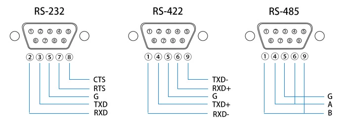
RS232 and RS422 are two other major serial communication protocols. While RS232 is limited in distance and device connectivity, offering point-to-point communication typically within 50 feet, RS485 extends this capability to 4000 feet and allows up to 32 devices on a single bus. RS422, similar to RS485 in terms of distance and voltage levels, differs primarily in its support for multi-drop configurations. RS422 is more suited for point-to-point or multipoint unidirectional communication, lacking the bidirectional, multi-drop capability inherent to RS485.
RS485 is the physical layer for several industrial protocols.
While RS485 inherently supports digital communication, it is often used in conjunction with analog-to-digital converters (ADCs) and digital-to-analog converters (DACs) to interface with analog sensors and control devices. This is useful when analog signals from sensors (like temperature, pressure, or flow sensors) need to be digitized for processing and monitoring in digital control systems.
Proper termination of the RS485 network is essential to prevent signal reflections, which can degrade communication quality. This involves matching the characteristic impedance of the cable with terminating resistors at each end of the network.
Cable selection and layout are also critical. Factors such as the type of twisted pair cable (shielded or unshielded), the environment where the cable is installed (including potential exposure to EMI), and adherence to proper grounding practices are critical for optimal network performance.
Maintenance of RS485 networks involves regular checks for any deterioration in cable integrity, connectors, and terminations. Additionally, Ensuring network reliability involves managing device limits and adhering to cable length specifications.

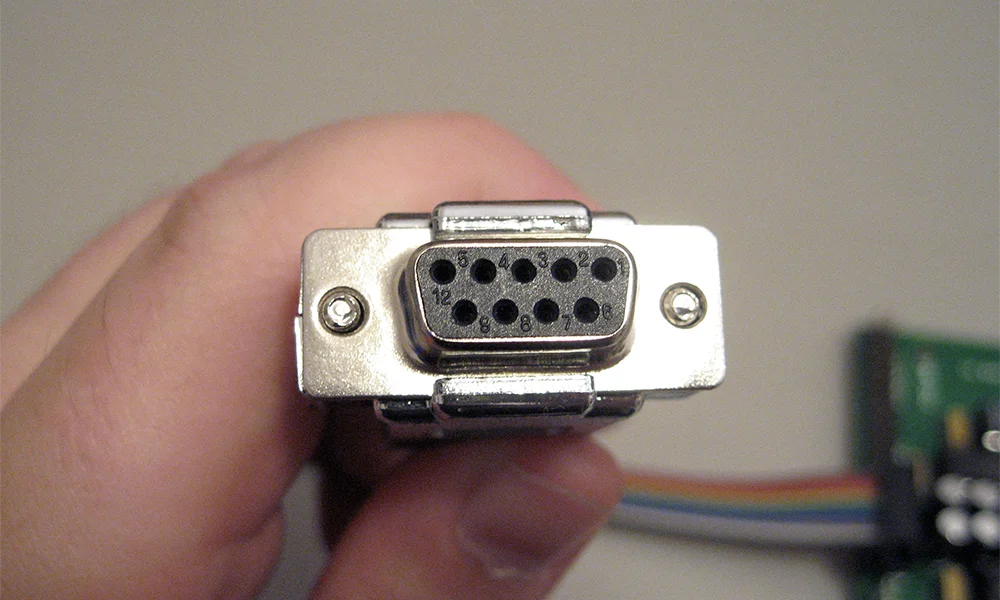
Despite newer technologies like USB and Ethernet, RS232 remains widely used due to its simplicity and broad compatibility. It's crucial in industries, scientific instruments, networking gear, and legacy computers. This protocol's reliability makes it the go-to for many applications. In this blog, we'll explore why RS232 continues to be relevant in our tech-savvy world.
Physical Characteristics of Connector Types (DB9, DB25)
The RS232 standard utilizes two primary types of connectors: DB9 and DB25.
Each connector type serves a specific application–modern, smaller applications or complex setups that need more control, respectively–with different pin configurations for transmitting data, receiving data, and various control signals.

Pinouts in RS232 connectors define the functionality of each pin. These configurations vary between DB9 and DB25 connectors. The standard pinouts include pins designated for Transmit Data (TXD), Receive Data (RXD), and several control signals like Request to Send (RTS) and Data Terminal Ready (DTR).
DB9 Pinout for RS232 Communication:
Despite the advent of more advanced communication protocols like USB and Ethernet, RS232 remains used due to its simplicity and wide compatibility. It's commonly used in industrial and scientific instruments, networking equipment, and legacy computer systems.
Common issues in RS232 communication include misconfigured baud rates, incorrect parity settings, and improper cable connections. Troubleshooting these problems requires a systematic approach, often involving checking cable connections, verifying device configurations, and using diagnostic tools like serial port monitors.

A voltage drop calculator is an essential tool for assessing the decrease in voltage across a conductor, ensuring electrical devices receive adequate power for optimal operation. Read our blog to learn more.
Voltage drop in electrical circuits can lead to various issues, affecting the performance and lifespan of electrical equipment:
Here's a table summarizing the NEC guidelines on voltage drop:
Voltage drop calculators typically require you to input the following parameters:
The calculator then computes the voltage drop based on the inputs and provides the result in volts or as a percentage of the initial voltage. Some calculators also provide the minimum conductor size required to limit the voltage drop to a specified level.
Voltage drop of the circuit conductors can be determined by multiplying the current of the circuit by the total resistance of the circuit conductors: The Ohm’s law (V = I*R) method only applies for DC current and cannot be used for three-phase circuits.
Transforming the formula, we have:
V = 2*R*I*L
Where:
Generally, with the cable information (length, size, material, operating temperature, and cover type), we can find its resistance and inductance from the reference tables. Three-phase AC power, with three sine waves offset by 120 degrees, is used in industrial and commercial settings for more efficient power distribution and to run heavy machinery.
V=3*I*L*(R*cosθ+X*sinθ)
For balanced three-phase circuits, a simplified calculation is:
V =3*I*Z*L/1000
Where:
The significance of calculating voltage drop extends beyond basic electrical design; it's a key factor in the overall performance and safety of electrical systems. Excessive voltage drop is a common culprit behind inefficient system performance, equipment malfunctions, and even safety hazards, which can lead to costly repairs and downtime. Furthermore, meeting the stipulations of electrical codes and standards, which dictate maximum allowable voltage drop levels, is non-negotiable for electrical professionals. Ensuring devices operate within these guidelines means that voltage drop calculations are not just a matter of efficiency but of compliance and safety as well.