In this post, we’ll show you exactly how to unlock the power of Flux Copilot for yourself: from writing rock-solid triggers to scoping entries at the project, user, and system levels.

This blog will explore functional block diagrams, their pivotal role in system design, the symbiotic relationship with ladder logic, structured text, and the broader realm of PLC programming. Why FBDs are so important within complex systems.
A functional block diagram is a schematic representation that delineates the principal functions of a system and the flow of data between them. It serves as a cornerstone in system engineering, simplifying the visualization of complex interactions within systems. FBDs are characterized by their use of labeled blocks connected by lines indicating dataflow, making them an intuitive means for depicting system operations.
The advantages of function block diagrams are that they’re very easy to follow and understand. They are generally laid out to mimic a specific process thus making it easy to understand for those who don’t have a background in plc programming.
In essence, an FBD breaks down large systems into manageable, functionally discrete blocks, facilitating a modular approach to system design. This modularity is crucial, allowing designers to focus on individual functions without being overwhelmed by the system's overall complexity.
The potency of a functional block diagram lies in its simplicity and clarity, achieved through three fundamental components:
FBDs do not exist in isolation; they are part of a larger ecosystem of programming languages and representation techniques used in the programming of programmable logic controllers (PLCs). Ladder logic, with its origins in electrical wiring diagrams, offers a graphical method that is intuitive for those with a background in electrical engineering. It depicts control logic in a format resembling a ladder, with rungs representing logical operations.
Structured text, another facet of PLC programming, is a high-level textual programming language that resembles traditional computer programming languages. It allows for complex instructions and algorithms to be implemented in a more familiar syntactic form.
FBDs complement these programming paradigms by providing a visual overview of system logic and dataflow, serving as a bridge between the conceptual design and the detailed implementation in ladder logic or structured text. This synergy enhances the understandability, development efficiency, and maintainability of PLC-based systems.
PLCs stand at the forefront of industrial automation, controlling machinery and processes with precision and reliability. In the domain of PLC programming, FBDs play a pivotal role, offering a graphical method for designing and implementing control logic.

FBDs align perfectly with the operational paradigm of PLCs, which are inherently designed to execute logic operations based on real-time data inputs. The visual nature of FBDs facilitates the rapid development and troubleshooting of PLC programs, enabling engineers to map out complex control strategies in a more intuitive and less error-prone manner.
Moreover, the adoption of FBDs in PLC programming underscores the importance of a clear and structured approach to system design. By visualizing the functional architecture of a system, engineers can ensure that all components interact harmoniously, leading to more robust and reliable PLC-based control systems.
As system complexity continues to escalate, the role of functional block diagrams in system design is not only preserved but also expanding. The integration of FBDs with advanced simulation tools and software development environments is enhancing their utility, allowing for more dynamic and interactive system modeling.
The future of FBDs is likely to witness further integration with artificial intelligence and machine learning technologies, enabling smarter and more adaptive systems. As these advanced systems become more prevalent, the clarity and efficiency offered by FBDs will become even more critical in navigating the complexity of modern system design.
Functional block diagrams are a testament to the power of visual representation in the realm of system design. By distilling complex system functionalities into comprehensible blocks and illustrating the dataflow dynamics, FBDs provide a foundation for designing, implementing, and maintaining sophisticated systems. Their symbiotic relationship with ladder logic, structured text, and PLC programming languages enhances their utility, making them an indispensable tool in the engineer's toolkit.
If you're a lover of smart home devices, you're likely buzzing with excitement over Arduino's recent collaboration with Silicon Labs. We are too, and we’re even more excited to bring the power of this collaboration to life on Flux. As of today, we’re excited to announce that engineers can fully design Arduino-based Matter boards with Flux.
The Matter protocol is growing to become a cornerstone of the Internet of Things (IoT) and smart home industries, offering a unified, secure, and reliable framework for connected devices. Developed by the Connectivity Standards Alliance (CSA), Matter was developed to simplify the complexity of IoT by ensuring that devices from various manufacturers can seamlessly communicate with each other.
At its core, Matter is an IP-based connectivity protocol that leverages common networking technologies such as Ethernet, Wi-Fi, and Thread to facilitate communication among smart devices. By adopting a universal approach, Matter enables devices to interact over existing networks, removing the need for proprietary bridges or gateways. This interoperability is achieved through a standardized application layer that operates on top of these networks, ensuring devices can understand each other regardless of the manufacturer. Even Zigbee devices can connect with Matter using a gateway device.
Prior to the introduction of Matter, the smartthings market was extremely fragmented, with myriad communication protocols leading to compatibility issues and a challenging user experience. Consumers would find themselves locked into a single ecosystem or struggle to integrate new devices into their existing setups. For example, a connected home might have to choose between Apple's ecosystem, with Siri, the Apple Homekit and the Homepod Mini, or Google's ecosystem, with Google Assistant, Google Home, and Google Nest. A smart plug that might support Amazon Alexa-enabled smart speakers might not support smart lighting from Nanoleaf.
Matter addresses these pain points by providing a common language for smart home devices, fostering an environment where products from different ecosystems can coexist and operate in harmony.
The news that has us so excited is Silicon Labs and Arduino’s recent partnership aimed at democratizing the IoT through the Matter protocol.
The partnership focuses on integrating Silicon Labs' advanced hardware with Arduino's extensive libraries and development environment to support Matter. On Arduino’s side, their team created a custom library and Arduino core for Matter-supported Silicon Labs microcontrollers. The major hardware involved in this partnership are Silicon Labs’ MG24 Series Wireless SoCs and the MGM240 Wireless Modules, as well as supported development boards including the xG24 Explorer Kit and the SparkFun Thing Plus Matter MGM240P.
Even more exciting is that, in the near future, the two companies will be releasing a brand new Arduino Nano board based around the MGM240 module.
Ultimately, the partnership is so important because it underscores the growing importance of Matter in the IoT and smartthings ecosystems. By combining Silicon Labs' cutting-edge wireless solutions with Arduino's accessible development tools, this alliance aims to empower developers, from hobbyists to professionals, to create innovative, Matter-compliant smart home products with ease.
Like the CSA, Flux is fully invested in democratizing technology. So now it’s Flux’s turn to contribute to the IoT community.
We’re excited to be supporting Arduino and Silicon Labs’ partnership by introducing a new Matter-compatible hardware lineup to the Flux community.
With available devices including the MG24 SoC, the MGM240 module, and development boards such as the xG24-EK2703A Developer Kit and the SparkFun Thing Plus Matter, Flux is your home for all things IoT. Not to mention our already-existing support for dozens of other components and modules from Arduino, Raspberry Pi, Seeed Studio, and more.
But sometimes, just having access to the parts is not enough. Ever stared at your Arduino, teeming with ideas but wondering, "Where do I even start?" We've all been there. But with Flux, those days are history.
Flux offers the perfect solution to significantly lowering the learning curve for hardware design. By providing reference designs and modules, and allowing users to fork and customize existing projects, Flux empowers designers to bring their unique IoT devices to life without ever having to start from scratch. Just Fork a project, tweak it, and boom—you're not just making a device, you're crafting the future.
So whether you’re a hobbyist developing a prototype for your smart home or you’re a seasoned professional building the next generation of home automation, anything is possible with Flux.
So, what are you waiting for? Dive into the exciting world of Arduino-based Matter projects with Flux. Bend the rules, break the mold, and bring your unique visions to life. We can't wait to see the magic you'll create with these new tools. Welcome to the future of IoT design, where your imagination is the only limit. Let's make something amazing together with Flux.
To learn more about Flux and the new Matter hardware, contact sales today!
This blog post explores the fundamental role of diodes in electronics, focusing on understanding their symbols and various types like Zener, Schottky, and LEDs. It details the electrical signal of diodes, illustrating how they allow current flow in one direction.
A diode, fundamentally a PN junction, permits current to flow primarily in one direction. It consists of two different doped semiconductor regions -- an N doped and a P dope region -- joined together, forming a PN junction.
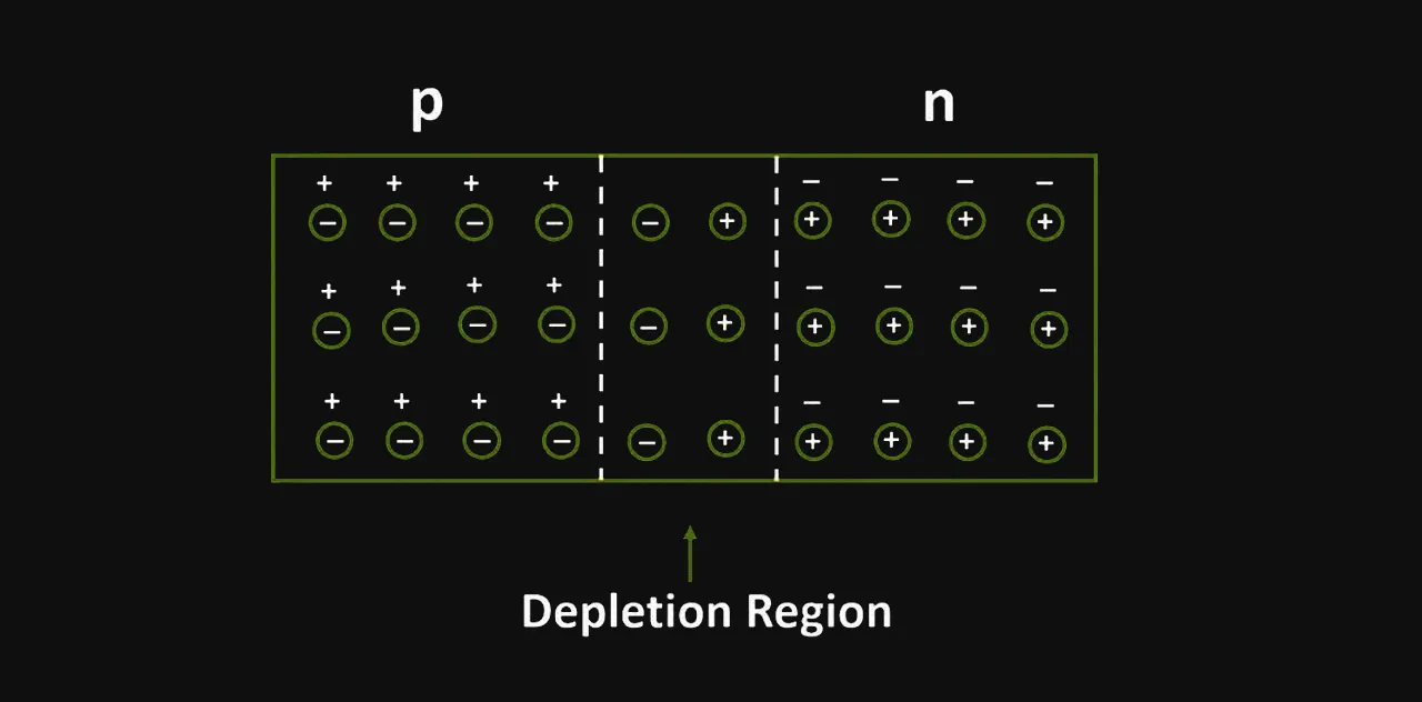
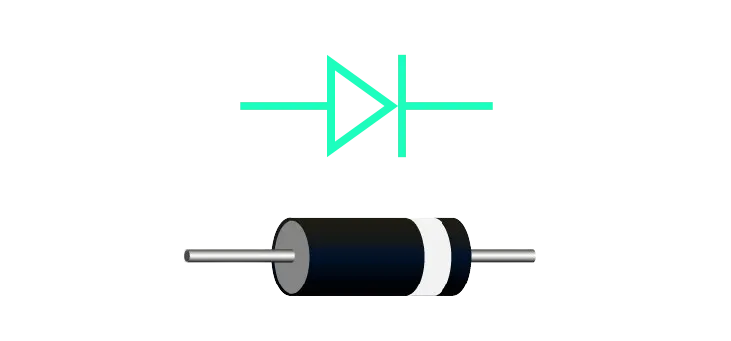
Its electrical signal is characterized by allowing easy current flow in the forward direction, while significantly impeding it in the reverse. This unique property is visually represented by an arrow, pointing in the allowed direction of current flow, and a line indicating the barrier for reverse flow.
Identifying a diode in a circuit involves looking for a component with two terminals: the anode and the cathode. The anode is marked by the arrowhead in the diode symbol, pointing towards the cathode, marked by the vertical line. Physical diodes often have a band on the cathode side. In schematics, diodes are also marked with designators like ‘D’ followed by a number (e.g., D1, D2).
Diodes serve myriad purposes in electronics. Their primary function is to enable unidirectional current flow, making them crucial for tasks like rectification – converting alternating current (AC) to direct current (DC). Specific diode types, such as the Zener diode, offer voltage regulation by maintaining a constant voltage over a range of currents. Varactor diodes (varicaps) change capacitance based on the applied voltage, useful in tuning circuits. Meanwhile, Schottky diodes, known for their low forward voltage drop, excel in fast-switching applications.
The function of a diode is primarily to control the direction of current flow in a circuit. Besides this, diodes have specialized functions based on their type:
A rectifier's core purpose is to convert AC to DC. In electronic circuits, this is crucial for powering devices that require stable DC voltage. Rectifier diodes are specifically designed for this task, efficiently handling high currents and voltages. Rectifiers are essential in power supplies, battery charging systems, and are integral to the functioning of electronic devices ranging from smartphones to industrial machinery.
In an automotive alternator, the rectifier converts the AC generated by the alternator into DC to charge the battery and power the electrical system. It typically employs a set of diodes arranged in a bridge configuration. The alternator generates three-phase AC, which the diode bridge rectifies into a smoother DC output. This process is vital for maintaining the battery’s charge and ensuring a consistent power supply to the vehicle's electrical systems.
Understanding diode symbols and their functions is a critical aspect of electronics. From simple rectification tasks to complex frequency tuning, diodes play pivotal roles in various applications. Recognizing these symbols not only aids in circuit analysis but also enriches the understanding of how electronic components interact to perform diverse and sophisticated functions. Whether it's a Zener diode stabilizing voltage or a laser diode in an optical communication system, each diode type brings unique capabilities to the vast and intricate world of electronics.
Designing a PCB is an intricate and engaging process that plays a pivotal role in electronics. The steps and tips provided in this article are not exhaustive but will certainly help you in your journey to designing effective and efficient PCBs. Armed with these insights, it's time to bring your electronic ideas to life with your own PCB designs
A PCB, or Printed Circuit Board, is a mechanically designed structure that electrically connects and mechanically supports electronic components using conductive tracks, pads, and other features etched from copper layers laminated onto a non-conductive substrate.
PCBs play a pivotal role in the functionality of virtually all electronic devices. They provide a physical platform for mounting components and establish the necessary electrical interconnections, thus forming a system's electronic circuitry.
The purpose of this article is to demystify the process of PCB design, taking you through the essential steps from conception to completion, along with offering practical tips for success.
The basis of any printed circuit board design lies in the electronic circuit you aim to build. Thus, a firm grasp of circuit design principles, such as understanding how different components interact and basic electronic principles, is vital.
Before starting the design, it is crucial to define the design parameters. These could include the board's size and shape, the number of layers, the types of components used (through-hole or surface mount), the operating environment, power requirements, and more.
Based on the design parameters and functional requirements, the right components and board material (such as dielectric) must be selected. Components should be chosen based on electrical requirements, availability, cost, and space considerations, while board material should provide appropriate thermal and mechanical stability.
The first step in PCB design is creating a schematic diagram that represents the electrical connections between different components. It serves as a blueprint for the PCB layout.
Each component symbol is placed on the schematic, and interconnections are drawn using lines to represent electrical connections or nets. Different components like resistors, capacitors, transistors, inductors, and integrated circuits, will each have their own unique component symbol.
The completed schematic diagram is used to generate a netlist, which is a comprehensive report detailing every electrical connection in the design.
Before progressing, the schematic should be thoroughly checked for errors to prevent problems in later stages.
Once the schematic is verified, the netlist is imported into a PCB layout tool to start designing the physical layout of the circuit board.
The PCB's dimensions and layers are defined, and design rules (spacing, width, etc.) are set based on manufacturing capabilities and requirements. This includes the selection of dielectric and stack up.

The completed schematic diagram is used to generate a netlist, which is a comprehensive report detailing every electrical connection in the design.
Before progressing, the schematic should be thoroughly checked for errors to prevent problems in later stages.

Components like capacitors, resistors, inductors, transistors, and integrated circuits are strategically placed on the circuit board to optimize space, minimize trace lengths, and avoid interference.
Traces, which are the copper paths connecting components, are routed based on the netlist. Their width is set to accommodate the current they will carry.
Unused areas on the PCB can be filled with copper pour to improve electromagnetic compatibility. Design rules checks (DRC) are run to ensure the design meets manufacturing tolerances.
Once the layout is finalized, Gerber files, which are the manufacturing blueprints for the PCB, are generated along with other manufacturing specifications.
The design is thoroughly reviewed one final time, and all necessary documentation for manufacturing is prepared.
The Gerber files and other documentation are sent to the manufacturer, and after their review and possible corrections, the PCB is manufactured. The manufacturer may also assemble the board for you, where they solder the electronic components.
Keep designs as simple as possible. Complexity increases the chances of error and can lead to difficulties in troubleshooting and manufacturing.
Constantly keep the design parameters in mind during the design process. Parameters such as operating frequency, power requirements, and environmental conditions can significantly affect the design.
Always be aware of the orientation of components, especially polarized components like diodes and capacitors, to avoid assembly errors. Appropriate designators on the silkscreen can help here. This can also help the assembly house when they solder the electronic components to the board.
Maintain clear and open communication with your PCB manufacturer. They can provide valuable feedback about design for manufacturability (DFM) and help avoid costly errors.
Designing a PCB is an intricate and engaging process that plays a pivotal role in electronics. The steps and tips provided in this article are not exhaustive but will certainly help you in your journey to designing effective and efficient PCBs. Armed with these insights, it's time to bring your electronic ideas to life with your own PCB designs!

Before you start this exciting journey, it's essential to equip yourself with the right knowledge, tools, and preparations. This article offers practical insights and suggestions to help you lay a strong foundation for your PCB design projects.
Throughout this article, I’ll also share with you various strategies and tips for surpassing the obstacles in your path. In today's digital age, where electronic devices have become an integral part of our lives, understanding the intricacies of PCB design is crucial for anyone seeking to create innovative and reliable electronic products.

PCB, short for Printed Circuit Board, is the backbone of virtually every electronic device we encounter today. Your iPhone has multiple of it, your laptop, your noise-cancelling headphones, your big flat tv, your smart watch, everything that are battery-powered devices for sure have one or more inside. PCB is a flat board made of non-conductive material, often fiberglass, with a layer of copper on one or both sides. The copper traces on a PCB act as electrical pathways, connecting various electronic components such as resistors, capacitors, inductors and complicated integrated circuits, and enabling them to work in harmony.
It is the critical bridge between the abstract world of circuitry and the tangible reality of electronic devices. Well-designed PCBs ensure the optimal performance, functionality, and reliability of electronic products. Whether it's a smartphone, a medical device, or a space exploration module, a thoughtfully designed PCB is the key to unlocking the full potential of the underlying electronics.
So, what factors should one consider before stepping into the fascinating world of printed circuit board design? While there are numerous aspects to keep in mind, let's highlight a few crucial ones. First and foremost, electrical performance takes center stage. The PCB design must account for signal integrity, power distribution, and electromagnetic compatibility, to prevent issues like signal degradation, voltage fluctuations, and unwanted interference.

But it doesn't end there. Mechanical aspects also play a vital role in PCB design. The size, shape, and mechanical support of the PCB are crucial factors in ensuring compatibility with the intended enclosure or system. Heat dissipation, component placement, and routing efficiency are all critical in preventing thermal issues and maintaining overall system reliability.
Manufacturability and cost-effectiveness should never be overlooked. Designing a PCB that should be easily fabricated, assembled (does it needs hot-air solder or just solder iron), and tested without compromising quality is essential for efficient production. Considering factors such as the vias spec, trace width and spacing, choice of dielectric materials, cores, component sourcing, and production techniques can significantly impact the overall cost and time-to-market of the final product.
When it comes to PCB design, the software or EDA/CAD you choose plays a vital role in the success of your design process. It can greatly impact the efficiency, accuracy, and overall quality of your final PCB layout. One EDA software that stands out in this regard is flux.ai. It offers a range of innovative features, including a community part library, a hardware AI assistant, and automated impedance control, making it a top contender worth considering.
What sets flux.ai apart is its integration of a hardware AI assistant, Flux Copilot. This advanced feature utilizes artificial intelligence to provide intelligent recommendations and guidance throughout your design journey. It's like having a knowledgeable companion by your side, helping you make informed decisions, optimize your designs, and minimize the chances of errors.
Another impressive feature of flux.ai is its latest feature: automated impedance control. This is particularly important in high-speed designs where maintaining signal integrity is crucial. By automating the impedance control process, flux.ai simplifies the task of achieving precise impedance matching. You just have to look for a component in the community library, add it to the schematic editor, and wire the pins together; then if the system detects you're using a component that needs impedance control - flux.ai will take care of the rest for you. This saves valuable time and effort for designers, allowing them to focus on other critical aspects of their design.
When selecting PCB design software, it's essential to consider your specific design requirements, ease of use, available features, and compatibility with your preferred design methodologies. It's also worth exploring the software's reputation within the industry, the level of community support, and the availability of comprehensive documentation. Altium Designer, Eagle, KiCad, OrCAD, and Proteus are a few examples of PCB design software out there.

At the core of every successful PCB design is the schematic diagram, sometimes called schematic design. It serves as the blueprint, visually representing the electrical connections and components of the circuit board design. A schematic diagram consists of component symbols, net connections between symbols, and netlist. These nets will become the traces on the PCB. The schematic diagram also acts as a common language, facilitating collaboration between engineers, designers, and manufacturers.
A well-designed schematic diagram brings clarity and organization to the circuit, allowing for a comprehensive understanding of its functionality. It also plays a vital role in ensuring electrical integrity by identifying and addressing potential issues early on, reducing the need for costly modifications later.
The schematic diagram serves as a reference point during testing and troubleshooting, enabling engineers to trace the signal flow and pinpoint problem areas. By utilizing standardized symbols and specialized software tools, the design process becomes more efficient and accurate.

In PCB design, layer stackup refers to the arrangement and configuration of the various layers that make up the PCB. It plays a crucial role in determining the performance, functionality, and manufacturability of the final board.
The layer stackup defines the number and type of copper and dielectric layers, their order, and the materials used. It directly impacts important aspects such as signal integrity, power distribution, thermal management, and impedance control. Proper layer stackup design ensures optimal electrical performance, reduces interference, and facilitates efficient routing of traces.
To create an effective layer stackup, designers must consider factors such as the number and types of signal layers, power, and ground planes, and the placement of critical components. The choice of materials for each layer and their dielectric properties is also significant, as it affects impedance matching, signal propagation, and heat dissipation.
By providing predefined layer stackups, Flux simplifies the design process and ensures compatibility with specific PCB manufacturers. The stackups configured for JLCPCB, PCBway, and AISLER, are tailored to their fabrication capabilities, including considerations for board thickness, copper weight, and minimum feature sizes. This facilitates seamless integration between the PCB design and manufacturing processes, streamlining production and reducing potential issues.
When working with flux.ai, designers can leverage the predefined layer stackups to align their design with the requirements of trusted PCB manufacturers. This not only saves time and effort but also enhances the likelihood of successful manufacturing outcomes.
In PCB design, one crucial aspect that greatly impacts the overall performance and manufacturability of the board is component placement. The strategic arrangement of components on the PCB plays a vital role in ensuring optimal functionality, signal integrity, thermal management, and ease of manufacturing and assembly.
Effective component placement starts with careful consideration of the functional requirements and constraints of the design. It involves placing components in such a way that minimizes signal interference, reduces trace lengths, and facilitates efficient routing. Proper component placement can enhance signal integrity by minimizing noise, crosstalk, and electromagnetic interference.
Thermal management is another critical factor to consider during component placement. Components that generate significant heat, such as power amplifiers or microprocessors, should be strategically positioned to allow for effective heat dissipation. Placing heat-sensitive components away from high-temperature sources can prevent overheating and ensure the longevity and reliability of the board.
Manufacturability and assembly considerations also come into play during component placement. Components should be positioned in a manner that allows for easy access during assembly and soldering processes. Adequate clearance and spacing should be provided to accommodate the size and shape of the components, as well as any required test points or connectors.
Coordinating the placement of PCB components with mechanical design elements, such as enclosure dimensions and mounting points, ensures seamless integration between the PCB and the overall product design.
To aid in efficient component placement, most PCB design software provides features like automated placement assistance and 3D visualization. These tools assist in aligning components, optimizing routing, and verifying clearances. However, the human touch and expertise of the designer remain invaluable in making informed decisions based on the specific requirements and constraints of the design.
In the world of PCBs, one critical aspect that demands careful attention and expertise is PCB routing. PCB routing involves the intricate task of connecting components and traces on the board, enabling the smooth flow of signals while considering factors like signal integrity, noise reduction, and manufacturability.
The routing process requires a keen understanding of the design requirements, electrical characteristics, and spatial constraints. Designers must carefully plan the routing strategy, taking into account the complexity of the circuit, signal frequencies, and the importance of signal paths.
To achieve optimal routing, designers must consider signal integrity factors such as trace length matching, impedance control, and minimizing electromagnetic interference. Critical high-speed signals often require controlled impedance routing, differential pair routing, and proper shielding techniques to ensure reliable signal transmission and prevent signal degradation.
Proper power distribution and ground plane design are also essential in PCB routing. By providing a robust power delivery network and a well-designed ground plane, designers can minimize voltage drop, reduce noise coupling, and ensure a stable power supply to all components.
While routing, designers must also consider the physical constraints of the PCB, including component footprints, board size, and mechanical considerations. Components should be placed and routed in a way that facilitates ease of assembly, maintenance, and future modifications if necessary.
Efficient PCB routing involves finding the optimal path for each signal while minimizing crosstalk and maintaining appropriate spacing between traces. Designers may employ routing techniques such as differential pair routing, length tuning, via stitching, and layer stacking to achieve the desired electrical performance.
Determining the appropriate trace width and spacing involves finding a balance between accommodating the current-carrying capacity of the trace, controlling impedance, and ensuring proper insulation between adjacent traces. The trace width refers to the width of the copper conductive path on the PCB. It plays a crucial role in carrying the required current without causing excessive resistance or voltage drop. Selecting the appropriate trace width depends on factors such as the maximum current expected to flow through the trace, the desired temperature rise, and the copper thickness. PCB Designers often refer to standard trace width tables or employ online calculators to determine the optimal trace width for a given current requirement.
Spacing between traces is equally important. It refers to the distance maintained between adjacent traces to prevent unintended coupling, crosstalk, and electromagnetic interference (EMI). Maintaining proper spacing ensures signal integrity and reduces the chances of cross-coupling between adjacent traces.
To establish appropriate trace width and spacing, industry standards and design guidelines are often followed. These standards specify minimum trace widths, spacing requirements, and clearance distances based on factors like signal type, operating frequency, and environmental considerations. Adhering to these guidelines helps ensure compliance with safety regulations and industry best practices.
One vital aspect that demands attention is understanding the design specifications for pads and vias. These elements serve as crucial connection points for integrated circuits, components, traces, and signal paths on the board. Having a thorough grasp of their design specifications is essential for achieving reliable electrical connections, efficient signal routing, and successful manufacturing.
Pads, also known as landing pads or soldering pads, provide the interface between the component leads and the PCB. They play a significant role in ensuring proper soldering, mechanical stability, and electrical connectivity. The design specifications for pads include dimensions such as diameter, shape, and solder mask clearance. These specifications are determined based on the component's footprint, lead size, and manufacturing process requirements.
The shape and dimensions of the pad should match the component's lead style, such as through-hole, surface-mount, or fine-pitch components. Adequate pad size and shape are crucial for achieving reliable solder joints and ensuring mechanical strength. The solder mask clearance around the pad helps to prevent solder bridging or short circuits during assembly.
Vias, on the other hand, are conductive pathways that connect different layers of the PCB. They enable the transfer of signals, power, and ground between different parts of the circuit. The design specifications for vias include parameters such as diameter, aspect ratio, and annular ring size.
There are different types of vias in PCB; through-hole via, blind via, buried via, and micro via. Through-hole vias are more common. Read more about different types of PCB vias.
The diameter of a via determines its electrical and thermal characteristics. It should be appropriately sized to handle the required current and ensure low-resistance connections. The aspect ratio, defined as the ratio of the via's depth to its diameter, affects the manufacturability and reliability of the via. Adequate aspect ratios are necessary to ensure proper plating and maintain structural integrity during the fabrication process.
The annular ring, which refers to the copper pad surrounding the via, is essential for maintaining the electrical connection between the via and the pad or trace. Sufficient annular ring width is necessary to ensure reliable electrical connectivity and prevent potential shorts or open circuits.

Gerber files are a collection of ASCII-based data files that describe the various layers, copper traces, pads, holes, and other design elements of the PCB.
When the PCB design is complete and ready for manufacturing, the design files are converted into Gerber files. These files provide a detailed representation of each layer of the PCB, including the top and bottom copper layers, solder mask layers, silkscreen layers, and drill files.
Gerber files are typically generated by the PCB design software used to create the layout. Each layer of the PCB design is exported as a separate Gerber file, with a specific extension that identifies the layer. The most common Gerber file extensions include .GTL (Top Layer), .GBL (Bottom Layer), .GTS (Top Solder Mask), .GBS (Bottom Solder Mask), .GTO (Top Silkscreen), .GBO (Bottom Silkscreen), and . TXT (Drill Files).
These Gerber files act as a bridge between the PCB designer and the PCB manufacturer. They contain all the necessary information required for the fabrication process, such as the dimensions, copper traces, solder mask openings, component placement locations, and drill hole positions.
Once the Gerber files are created, they are typically bundled together and submitted to the PCB manufacturer for the manufacturing process. The manufacturer uses the Gerber files to generate the photolithographic films or digital equivalents that are used in the fabrication steps, including the creation of the copper layers, solder mask application, silkscreen printing, and drilling of holes.
The BOM specifies the quantity of each component required for the PCB assembly, enabling accurate procurement and inventory management. The reference designator assigns a unique identifier to each component on the PCB, facilitating proper placement and soldering during the assembly process.
Finding a reliable and suitable manufacturer ensures the successful fabrication of your PCB design.
Choosing the right PCB manufacturer involves considering several factors. Here are a few key points to keep in mind:
So, are you ready to take the first step towards your PCB project? Turn your ideas into tangible circuit boards that can make a difference whether it's for your hydronics system, automated curtain opener, IoT-based projects or designing hardware for the next SpaceX mission, Flux is where great hardware projects are born. Get started now for free!
In this article, we will discuss the key components of the Arduino Uno schematic, including the microcontroller, voltage regulator, USB interface, and passive components, and how they work together to make the board work.
The following Arduino Uno schematic diagram can be opened and forked in Flux so that you can create your own custom layout! This allows you to modify the position of components while maintaining the same pinouts.

The Arduino Uno schematic consists of several components, including the microcontroller, voltage regulator, USB interface, and various other passive components. Let's take a closer look at each component and its function in the schematic.
The Arduino Uno schematic provides a comprehensive pinout that gives electrical engineers access to various peripheral interfaces, such as I2C, SPI, and PWM. To utilize these interfaces, electrical engineers must first set the appropriate pinmode using the pinmode function. This function specifies whether a pin is set to input or output, which determines its behavior. The pinout of the Arduino Uno also includes connections to the GND and 3V pins, which are used to provide power to external devices and to ground the board.
The Arduino Uno consists of a total of 20 digital pins, 6 of which can be used for PWM output, and 6 analog input pins. The pinout also includes connections to the power supply, including the GND and 3V pins, as well as a number of other peripheral interfaces, such as I2C and SPI.
Digital Pins
The digital pins on the Arduino Uno can be used for both input and output and are designated as D0 to D13. These pins can be controlled using the digitalwrite and digitalread functions in the Arduino IDE.
Analog Pins
The analog pins on the Arduino Uno are designated as A0 to A5 and can be used to read analog signals, such as those from sensors. These pins are connected to an ADC (Analog-to-Digital Converter) on the ATmega328P microcontroller, which converts the analog signal into a digital representation that can be read by the microcontroller.
PWM Pins
The Arduino Uno provides 6 PWM pins, which can be used to control analog devices, such as motors and LEDs, by adjusting the duty cycle of a pulse. These pins are designated as D3, D5, D6, D9, D10, and D11.
I2C and SPI Interfaces
The Arduino Uno pinout also includes connections to the I2C and SPI interfaces, which allow electrical engineers to communicate with other devices and peripherals, such as sensors and actuators.
Power Pins
The power pins on the Arduino Uno include the GND and 3V pins, which are used to provide power to external devices and to ground the board. The 5V pin provides a regulated 5V supply, which can be used to power external devices, while the Vin pin can be used to power the board using an external power supply.

The ATmega328P microcontroller on the Arduino Uno is programmed using the ICSP (In-Circuit Serial Programming) header. This header provides access to the MOSI, SCK, and other signals required for programming the microcontroller. The Arduino Integrated Development Environment (IDE) provides an easy-to-use interface for programming the microcontroller and uploading code to the board.
The Arduino Uno schematic provides access to 14 digital pins, which can be used to control various devices, such as LEDs and sensors. Electrical engineers can use the digitalwrite function to set the state of a digital pin to either high or low. The state of the digital pin can be read using the digitalread function, which returns a value of either 0 or 1, depending on the state of the pin.
This example Arduino code shows how to control digital pins using digitalWrite() and digitalRead() functions. In this example, we'll use a push button to control an LED. When the button is pressed, the LED will turn on; when the button is released, the LED will turn off.
This code assumes that you have a normally open push button connected to digital pin 2 and an LED connected to digital pin 13. When the button is not pressed, the internal pull-up resistor will cause the button pin to read HIGH. When the button is pressed, it will connect the pin to ground, causing the pin to read LOW.
The Arduino Uno schematic provides access to 6 PWM (Pulse Width Modulation) pins, which can be used to control analog devices, such as motors and servos. PWM allows electrical engineers to control the brightness of LEDs, the speed of motors, and other devices by adjusting the duty cycle of the pulse. This provides a more versatile and smooth control of analog devices compared to using digital signals alone.
In this example, we'll use a potentiometer to control the brightness of an LED. The potentiometer will be read using an analog input, and the LED brightness will be controlled using a PWM output.

There are several ground (GND) pins on an Arduino Uno board. Typically, you can find at least 4 GND pins located on the board's power and ground bus along the edges of the board. These pins are labeled "GND" and are used to connect components to a common ground and complete the electrical circuit.
The "0" and "1" pins on an Arduino Uno refer to the RX (Receive) and TX (Transmit) pins, respectively. These are digital pins used for serial communication with other devices, such as a computer. The RX pin is used to receive data, and the TX pin is used to transmit data. These pins can also be used for general digital input/output if serial communication is not required.
The Arduino Uno can be used in various applications, including hobby projects, IoT devices, and home automation. Engineers and hobbyists can use the schematic as a reference to create custom boards or modify existing boards to meet specific requirements. The schematic can also be used to troubleshoot issues with the board and to understand the behavior of the components.
One of the most significant advantages of using the Arduino Uno is its compatibility with the Arduino Integrated Development Environment (IDE). The Arduino IDE is a software platform that makes it easy to write, upload, and debug code for the Arduino Uno and other boards. The Arduino Uno schematic can be used in combination with the Arduino IDE to create and test new projects, making it an ideal choice for hobbyists and engineers.
The schematic of the Arduino Uno is an essential tool for electrical engineers and hobbyists to understand the behavior of the board and to modify it for specific projects.