This update brings more than just polish—it’s the foundation for a faster, more fluid design experience, built around the way Copilot is used today and the way we see it evolving tomorrow.
KiCad revolutionized PCB design by making it accessible to everyone. Flux builds on that foundation, offering a browser-based, AI-powered platform that takes your PCB design experience to the next level.
If you’re a KiCad user considering a switch to Flux, you might be wondering how the two platforms compare. To help you decide, we’ve broken down the key differences that set Flux apart from KiCad and how it can streamline your design process.
In KiCad, it can take a while to configure your project to get started. Even when you find a reference project, you still need to go through several steps to import the project, libraries, and everything you need get going.
In Flux, all you have to do is open a new project and everything is ready to go! What’s more - all public projects, parts, and modules can be forked and built upon with the click of a button. Similar to GitHub, Flux has been built with reusability in mind from the very beginning.

In KiCAD, library management, schematic editing, PCB editing, and simulation can feel like completely different flows. That can make it hard to keep track of everything and make sure your project stays in sync.
In Flux, the schematic editor, BOM, PCB editor, and simulator all work in one workflow that stays in sync in the browser. There’s also a version control system that makes it easy to revert changes.
In KiCad, you have to maintain multiple libraries which can become extremely time-consuming to keep up to date. When sharing KiCAD designs sometimes projects will break because the reference library isn’t linked.
In Flux, there’s a single unified library that’s being constantly updated and improved upon by the community. This allows you to easily use other people’s vetted parts instead of making your own.

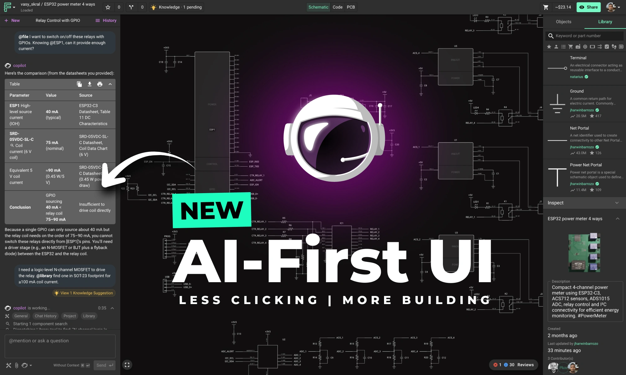
Flux Copilot is the industry's first AI-powered hardware design assistant integrated into a PCB design tool. With its ability to understand schematic designs, component lists, connections, and part information from datasheets, Copilot offers a wealth of knowledge and capabilities that can transform the way hardware design is approached.
In KiCAD, files remain on your computer and sharing and getting feedback often involves sharing screenshots via emails and Slack conversations. Version control is also very difficult, especially when working with others.
In Flux, sharing with contractors, collaborators, clients, and other stakeholders is as easy as sharing a link.

With KiCAD, like all open source software, there is support by community members & contributors which is awesome! However, without centralized support, fixes and features can take easily up to a year.
With Flux, you have access to browser-based software where fixes and new features are instantly deployed to all users and a platform that’s updated frequently based entirely on your feedback.
Making the switch to Flux is easy. Create a Flux account, follow the KiCad to Flux migration tutorial to get your projects into Flux, or follow this video tutorial:

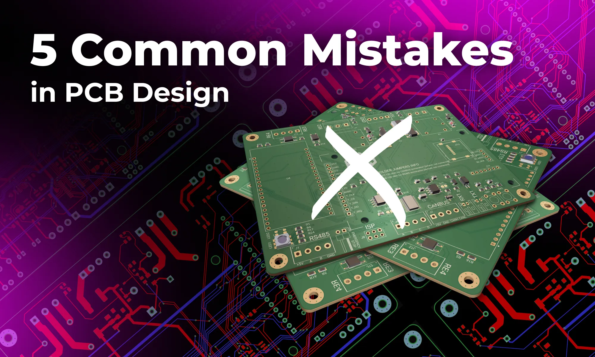
In this post, we’ll explore five common mistakes companies make when contracting PCB design and how you can avoid them by using tools like Flux to keep your project on track, from concept to completion.
PCB design is complex, and when you’re relying on external partners, even small missteps can lead to costly reworks, missed deadlines, or designs that aren’t manufacturable. Luckily, many of these headaches can be avoided with the right tools and practices.
In this post, we’ll explore five common mistakes companies make when contracting PCB design and how you can avoid them by using tools like Flux to keep your project on track, from concept to completion.
One of the biggest mistakes teams make when outsourcing PCB design is failing to set clear, detailed goals from the start. Without well-defined functional requirements, timelines, budgets, and constraints, it’s easy for the project to drift off course, leading to miscommunication and unmet expectations.
Clear goals ensure that both you and your contractor are aligned from day one. Without them, you risk costly delays, unnecessary revisions, and potentially ending up with a design that doesn’t meet your needs.
While clear requirements are critical, it’s also important to give the contractor room to innovate where it makes the most impact. For instance, allow flexibility in areas like power optimization, component placement, or alternative materials, so long as they meet the core functional requirements.
By using a tool like Flux, you can streamline this process even further. We’ve created a Flux Project Requirements Template that includes all the properties you need to define your PCB design requirements. This not only makes it easy for contractors to fill out, but Flux Copilot can also use these inputs to evaluate designs in real-time, ensuring your goals are met without constant back-and-forth.
{{insert-project-requirement-template}}
Providing your contractor with a head start can make a huge difference in the success of your PCB design project. When you give them initial drafts, prototypes, or even early design ideas, it helps your contractor understand your vision more clearly, accelerates the process, and allows them to provide better insights from the outset.
By offering them something to build on, you create a collaborative dynamic where the contractor can refine your ideas rather than starting from scratch. This not only saves time but also leads to a more aligned and higher-quality end result.
Communication is essential for any contracting relationship, but especially so in PCB design. Without regular check-ins and updates, issues can slip through the cracks, leading to costly revisions and delays later on. Frequent communication ensures that everyone stays on the same page, allowing you to catch potential problems early and keep the project moving forward smoothly.
The more you communicate, the better the end result will be. Contractors rely on your feedback and direction to align their work with your expectations, so regular updates are essential.
Scope creep is one of the biggest threats to PCB design timelines. It's easy to add more features as the project progresses, but this often leads to delays, increased costs, and a more complicated design than initially intended.
By limiting the scope, you allow your contractor to deliver a usable, testable design in a shorter time frame, which you can iterate on based on real-world feedback. This approach minimizes risk and helps you avoid being stuck in long design cycles.
The tools you use to manage the PCB design process can make or break the success of your project. Without the right platform to set goals, manage versions, and facilitate communication, it’s easy for things to go off track. Miscommunication, outdated files, and scattered feedback can lead to confusion and delays. Using the right tools helps streamline collaboration, ensuring that everyone involved in the project is working efficiently and with the latest information.
{{insert-nico-video}}
Choosing a tool that supports seamless communication and version control can significantly reduce the friction that often occurs during outsourced PCB design.
By avoiding these five common mistakes and utilizing the powerful capabilities of Flux, you can transform how you approach contracting PCB design. With clearer communication, faster iterations, and smarter design tools, you’ll not only save time but also ensure a successful outcome for your project. Sign up for Flux today!
Learn how smart vias in Flux automates the selection, placement, and configuration of vias during the PCB design process. This automation reduces the manual effort involved in via placement and significantly lowers the risk of misalignment and other common errors associated with traditional via management.
Even for the most experienced engineers, high density interconnect designs remain difficult. Some typical challenges are:
Traditional EDA tools depend heavily on manual input for via placement. This makes density management primarily a function of hand-eye coordination. After placement, when you need to modify part of the design, you’ll quickly find yourself playing an unsolicited game of three-dimensional chess. Often, it’s easiest to simply wipe out the traces and vias, start over, and hope you won’t have to make another change to that part of your board.
After carefully laying everything out, the next big effort is to define and work through manufacturability, reliability, and cost considerations. In practice, this mountain of manual labor adds up. Designers are often forced to either compromise their design, risk overlooking mistakes, or delay their project.
Smart Vias in Flux is an intelligent feature that automates the selection, placement, and configuration of vias during the PCB design process. This automation reduces the manual effort involved in via placement and significantly lowers the risk of misalignment and other common errors associated with traditional via management
If you’re routing a trace and need to connect across multiple layers, Flux will place a Smart Via that automatically populates with the best suited combination of vias (micro, blind, buried, or through-hole), in a stacked or staggered configuration, respecting your project settings. For example, you might only want to use microvias on outer layers and use through-hole vias for everything else. With Smart Vias, you can just start routing. When you switch from Top to Mid-Layer 1, a Smart Via will get you there. You can change your mind and go to Bottom and the Smart Via will dynamically reconfigure itself to support that connectivity.

Smart Vias are powered by Flux’s innovative Layout Rules. Rules allow you to set your preferences from a central place in the Stackup. They also allow for control of individual Smart Vias right down to the details, like the direction or spacing of a stagger. The result is a feature gets out of your way when you want and also lets you sweat the small stuff.
To make it even easier to get started, simply clone or fork any of these templates.
Overall, Smart Vias addresses many of the challenges inherent in high density interconnect design and offers notable benefits to the designer.
We think this is a huge improvement over existing workflows and we’re excited for you to use it. Interested in experiencing the new Smart Via feature? Get started with a template today!
Avoid costly errors in your PCB design with these expert tips! Discover the 5 most common mistakes in trace width, vias, power planes, and more. Learn how Flux’s AI Copilot helps you catch these issues early, ensuring your board is ready for manufacturing.
Let's dive in.
One of the most common mistakes in PCB design is not paying enough attention to trace width and spacing, especially in high-current or high-speed applications. If the trace is meant to carry high currents but it happens to be too narrow, it can result in thermal issues or even a failure of the circuit.
The width of your trace can be determined by things like; how much current it should carry without overheating or causing excessive voltage drops, Impedance control, and sensitivity of the signal running through it.
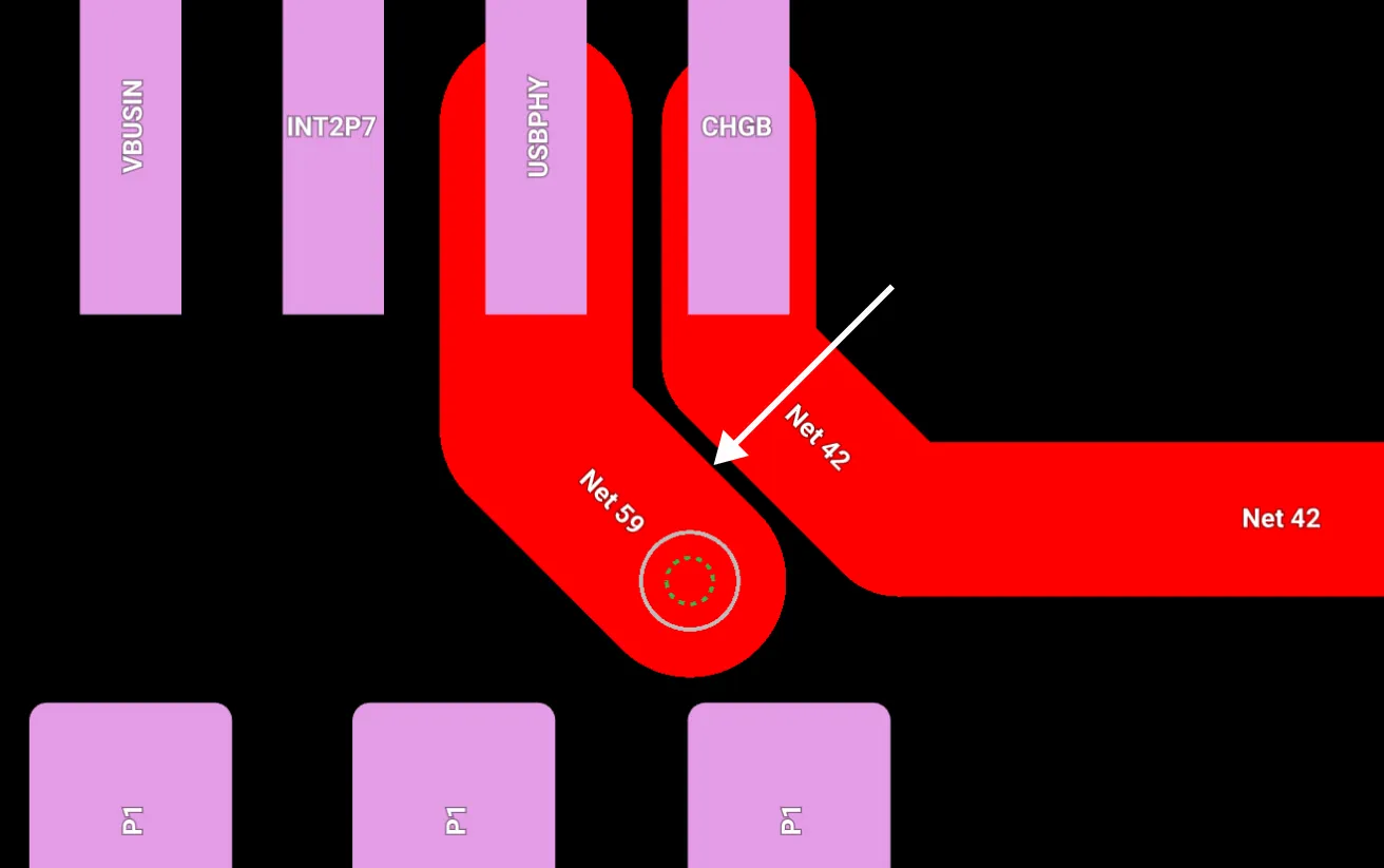
Flux makes routing high speed signals, such as USB data lines, easier by automatically performing coupled routing of the data lines (D+ and D-) and calculating the impedance of the pair based on the PCB stackup. This helps prevent reflections that can cause signal distortion, timing issues, and data corruption.
Flux Copilot can also help you calculate the appropriate trace width based on the current it needs to carry, while also considering the required impedance for high-speed signals. Just ask something like:
@copilot please recommend trace width for my VBUS.
Then copilot responses:
“For VBUS, typically a 5V supply in USB applications, let's assume a common scenario where you might anticipate a current of up to 1A. Using a temperature rise of 10°C, the general guideline for trace width on a 1 oz/ft² copper PCB is approximately 20-30 mils (0.5-0.8 mm) per amp of current.”
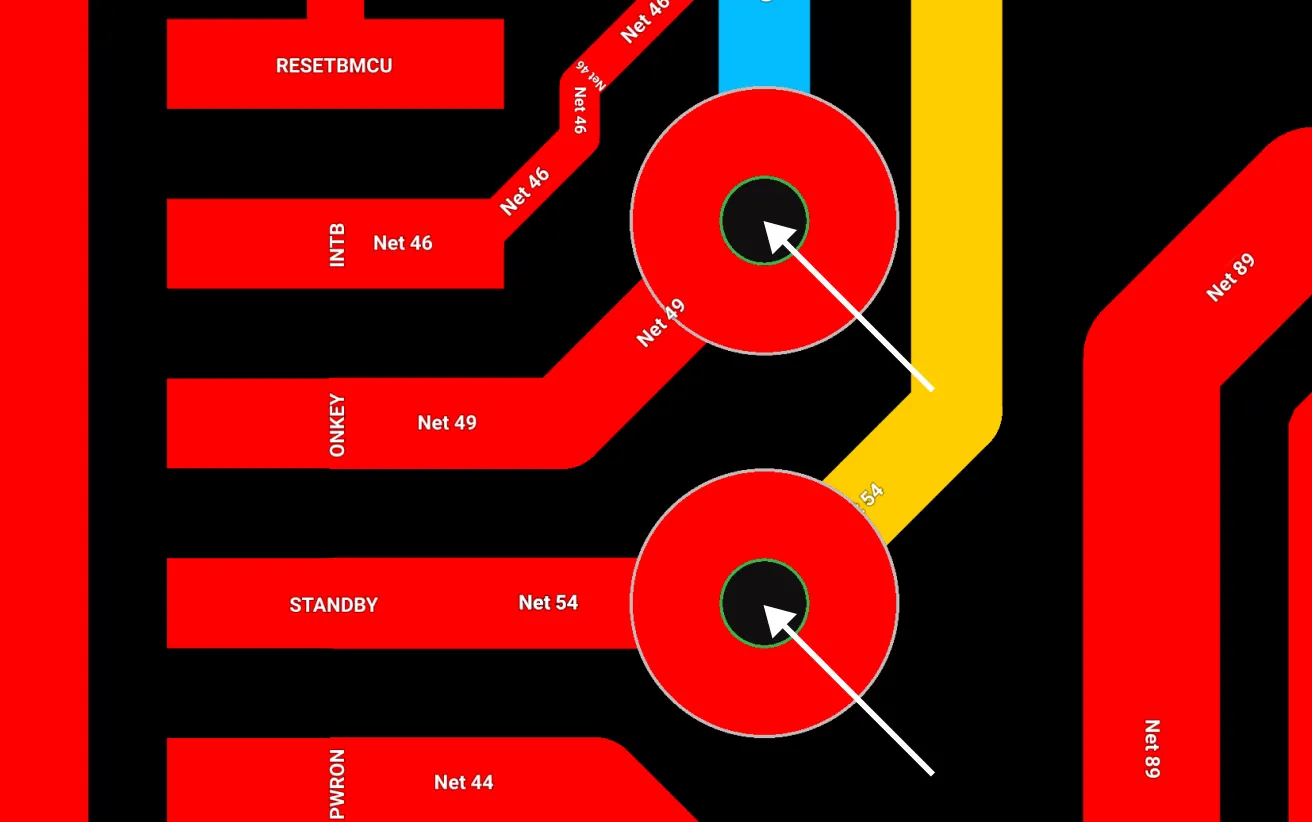
Vias are crucial for connecting different layers in a PCB, but choosing the wrong size or type can cause issues in both signal integrity and manufacturing. Blind, buried, and microvias are often used in high-density interconnect (HDI) boards, but these require careful consideration during design. For instance, microvias are perfect for compact designs, but if placed improperly, they can lead to poor layer transitions or increased inductance.
Flux let’s you set up your stackup where you add all the manufacturer capabilities. When you need some more advice on what stackup best suits your design, always feel free to ask copilot for some ideas, you could ask
@copilot in a table format recommend vias sizes that i can use for my VDD3V3, my USB, and the other signal buses?
Then here's the copilot response,
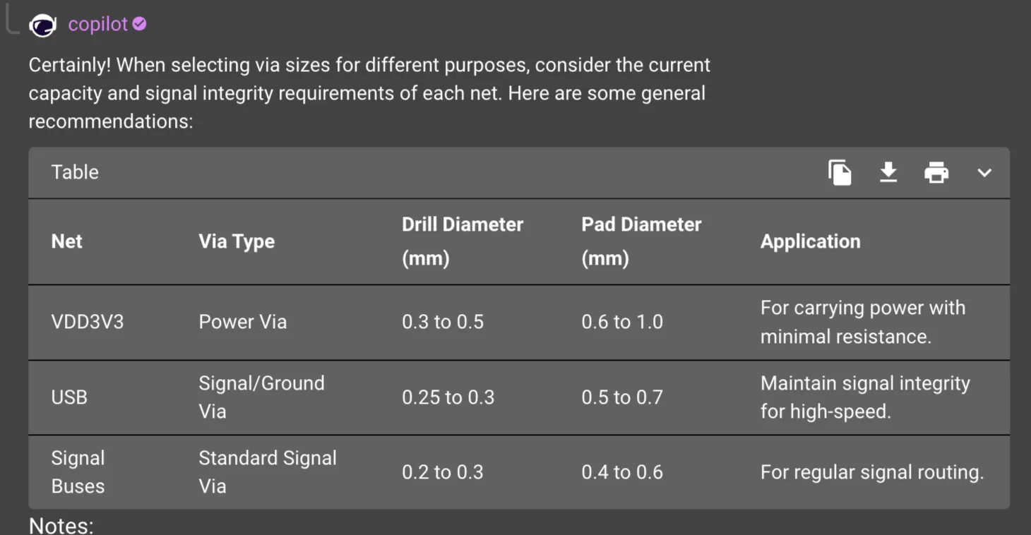
If you're routing a high-speed differential pair, such as USB or PCIe, through multiple layers, via stubs can cause signal reflections that degrade signal quality. A rule of thumb is to ensure via lengths are minimized, or even better, use back-drilling techniques to remove stubs, especially in high-frequency circuits.
Moreover, not all manufacturers support the same via sizes, so checking with your manufacturer early in the design process can avoid headaches later. Make sure to adhere to their capabilities, including the aspect ratio limits (via depth to diameter), to avoid costly redesigns e.g. 20:1 for PCBWay.
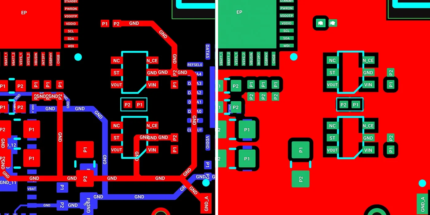
The layout of power and ground planes is another common area where mistakes are made. These planes act as the backbone of your circuit's stability, so a poorly designed plane can introduce noise, increase EMI, and degrade power delivery.
By default, Flux starts you off with a solid, contiguous ground plane since it is critical for minimizing noise and providing a low-impedance return path for high-speed signals. It is advisable to avoid creating islands which can cause severe signal integrity.
Example:
Imagine routing a high-speed signal across a split ground plane. The signal may cross the gap, creating a longer return path, which increases inductance and can lead to signal distortion or timing errors in critical circuits like clocks or data buses.
Similarly, power planes should be wide enough to handle the current required by each section of the circuit. For designs with sensitive analog circuits, it’s often a good idea to have separate power planes or split planes for analog and digital sections to avoid cross-talk and noise coupling.
Designing with manufacturability in mind is essential to ensure that your board can be built without issues. It’s easy to forget that the design rules you use in your ECAD tool may not fully align with your manufacturer’s capabilities, and this can result in delays or additional costs.
Flux provides users with pre-configured templates which align with most of the popular manufacture (e.g. PCBWay, JLCPCB, AISLER, LION Circuits, SEEED Studio and many more) capabilities so that users don’t have to worry about manually configuring things like trace widths, keepout, and other parameters. A good general rule of thumb is to always start new project using Flux manufacturer design rule templates
There are numerous DFM tips but here are some common ones to consider;
Using Flux manufacturer design rule templates will alert you when either of the manufacturer capabilities are violated even before sending your files for manufacturing saving you time.
Decoupling capacitors are used to filter out noise and provide a stable voltage to ICs, especially in digital circuits where rapid switching causes power fluctuations. However, placing these capacitors too far from the pins of the IC can render them ineffective. It is advisable to place these decoupling capacitors as close as possible to the IC without violating the minimum spacing a manufacturer can work with.
Example:
In a typical microcontroller design, you should place decoupling capacitors (such as 0.1µF and 1µF) as close as possible to the VCC and GND pins. Ideally, the capacitors should be placed on the same layer as the IC to reduce parasitic inductance and ensure faster response times. Failure to do so can cause power integrity issues, leading to glitches or resets in your circuit.
Additionally, use vias sparingly when routing decoupling capacitors. Each via adds inductance to the path, which reduces the capacitor's ability to suppress high-frequency noise.
Before pressing that button to send your PCB design for manufacturing, it's worth taking a step back and performing a thorough review of your design. These design review steps can be quite a handful but what we have discussed above can be considered as the bare minimum. Flux manufacturer design rules makes it easy to ensure trace widths, appropriate via sizes, and manufacturer capabilities are considered when designing your board.
A thorough PCB design review can be a very daunting task, you might not be sure where to start or what checks to include in the review process. That is one of the reasons Flux’s AI lives in your project. You can use copilot to quickly check decoupling capacitors, power and grounding, ensuring compliance with industry standards, and even creating a stronger supply chain. To learn more about how you can use this tool, Sign up for Flux today.
Learn about STM32 microcontrollers, popular series, USB OTG, SWD, UART, and development tools. Find the right STM32 MCU and kickstart your projects.
A typical microcontroller includes a processor, memory and Input/Output (I/O) peripherals on a single chip. Its components may be extended to include: Digital I/O, Analog I/O, Timers, Communication interfaces, Watchdog (a timer that is responsible for the detection of timed out or locked instruction).
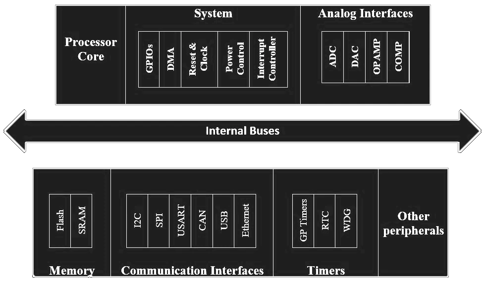
A processor is a little chip present in the device that has the role of arranging the instructions and order the outputs. The manufacturer defines the integrated peripherals and the hardware capabilities.
STM32 microcontrollers are divided into several groups based on their target applications. Below is a quick overview to help you choose the right MCU series:
{{insert-project-1-here}}
There are two ways to use an STM32 MCU which are:
{{insert-project-2-here}}
STM32 microcontrollers come equipped with several critical features that make development smoother, especially for embedded applications. Here are a few that stand out:
{{insert-project-3-here}}
To get started with STM32, you’ll need a development board. Here are some of the top picks, whether you’re on a budget or seeking advanced features:
Once you’ve chosen a development board, the next step is setting up the software. Below are some of the best free IDEs and tools to get started with STM32 programming:
For IoT projects, consider Arm Mbed, a platform that supports cloud-based development and is optimized for low-power devices.
STM32CubeMX simplifies the configuration process by generating initialization code. You can:
Create a basic “blinky” program to blink an LED. This is a great way to ensure everything is set up correctly.
{{insert-mark-video}}
You can find STM32 MCUs and development boards from trusted vendors, such as:
STM32 microcontrollers are an excellent choice for both beginners and advanced developers. They offer a wide range of features, low power consumption, and support for IoT, wireless communication, and industrial automation. With STM32Cube tools and free IDEs, you can build your projects faster and more efficiently.
Whether you’re working on a simple blinky LED project or a complex IoT solution, STM32 has the right series to fit your needs. Get your development board, set up your environment, and start building today!
Q: What is the best STM32 series for beginners?
A: The STM32F1 and STM32F4 series are great starting points, as they are well-documented and widely supported.
Q: Is STM32CubeIDE free?
A: Yes, STM32CubeIDE is free and available for Windows, macOS, and Linux.
Q: How much does an STM32 microcontroller cost?
A: Prices vary by series, with the STM32F1 starting around $2 and high-end STM32H7 costing up to $30.
Q: Is STM32 better than Arduino?
A: While Arduino is simpler and more beginner-friendly, STM32 offers more power, flexibility, and scalability. STM32 microcontrollers provide better performance with faster processing speeds, more peripherals, and lower power consumption, making them ideal for more advanced or professional projects. On the other hand, Arduino is great for quick prototyping and those new to microcontrollers.
Q: What are STM32 microcontrollers used for?
A: STM32 MCUs are used in a wide range of applications, including IoT devices, automotive systems, industrial automation, wearables, and smart home products. Their versatility makes them suitable for both high-performance tasks (like multimedia processing) and low-power applications (like battery-operated devices).
Looking for a comprehensive guide to ESP8266 pinout? Check out our article that covers everything you need to know about the ESP8266's pins, including digital, analog, and PWM pins. Perfect for beginners and experts alike, our guide will help you understand the ESP8266's pinout and how to use it in your projects.
In this guide, we’ll walk through:
The ESP8266 is a low-cost Wi-Fi microcontroller by Espressif. It enables wireless IoT projects without needing a separate Wi-Fi module. Popular boards like the NodeMCU and Wemos D1 Mini use it as their core.
The ESP8266 microcontroller module features a total of 32 pins, each with a function that contributes to its remarkable utility. Here, we'll break down these key specifications to provide a clear understanding of its pinout:
The ESP8266 features 32 pins, but not all are usable for general I/O. Here’s a breakdown:
You can power ESP8266 directly via the USB connector (standard USB = 5V) or the Vin pin (5V to 10V). The regulator provides a maximum of 500mA.
These are the power pins of this microcontroller board:
It's essential to realize that the GPIO labeling on the ESP8266 does not correspond directly to the silkscreen markings on the board. For instance, the pin marked as D0 is actually GPIO16, while the one labeled D1 is in fact GPIO5.
The table below outlines the relationship between the silkscreen labels on the board and the actual GPIO numbers, detailing the most suitable pins for your projects and highlighting those that require careful handling.
GPIO6 to GPIO11 are usually connected to the flash chip in ESP8266 boards. So, these pins are not recommended to use.
The ESP8266 can be prevented from booting if some pins are pulled LOW or HIGH. The following list shows the state of the following pins during BOOT:
{{insert-project-1-here}}
ESP8266 only has one analog input, it's the ADC0 pin, usually labelled as A0 on the board. If you're using the bare ESP8266 chip, the maximum input voltage range of this ADC0 is 0 to 1V, for development board like NodeMCU ESP8266 12-E, the voltage input range is 0 to 3.3V due to presence of internal voltage divider.
This ADC pin has a 10-bit resolution, which means you’ll get values between 0 and 1023.
Unlike other microcontrollers, the ESP8266 lacks dedicated hardware for I2C; however, I2C functionality can be implemented in software, allowing any GPIOs to be used for I2C purposes. Commonly, the following GPIOs are used as I2C pins:
The pins used as SPI in the ESP8266 are:
The ESP8266 supports interrupts in any GPIO, except GPIO16.
The GPIO pins on the esp8266 are the backbone of its versatility, allowing you to connect various components to create a wide array of IoT applications. To illustrate their practical utility, let's consider a simple project: building a weather monitoring station.
And with the many additional pinouts, our weather monitoring station can always be improved--add a temperature sensor to GPIO2, or a humidity sensor to GPIO3!
{{insert-project-2-here}}
The esp8266 pinout is also perfect for developers who are already comfortable with the Arduino IDE, as they seamlessly integrate, making the esp8266 widely accessible.
Using the Arduino IDE with the esp8266 offers several benefits:

When it comes to practical application, the Wemos D1 Mini, built around the esp8266, is a favorite among developers. Its compact size, affordability, and extensive support from the maker community have made it a go-to choice for IoT projects.
Here are some reasons why the Wemos D1 Mini is an excellent choice:
In the evolving landscape of IoT, the esp8266 pinout is highly versatile. Its GPIO pins, compatibility with Arduino IDE, I2C capabilities, and integration into popular development boards like the Wemos D1 Mini provide a robust foundation for your IoT projects. However, if you're looking for something more, then check out its sibling, the esp32. The esp32 retains the flexibility of the esp8266 pinout while offering more processing power, built-in Bluetooth, and dual-core processing. This opens up new opportunities for more complex and feature-rich IoT applications.