In this post, we’ll show you exactly how to unlock the power of Flux Copilot for yourself: from writing rock-solid triggers to scoping entries at the project, user, and system levels.
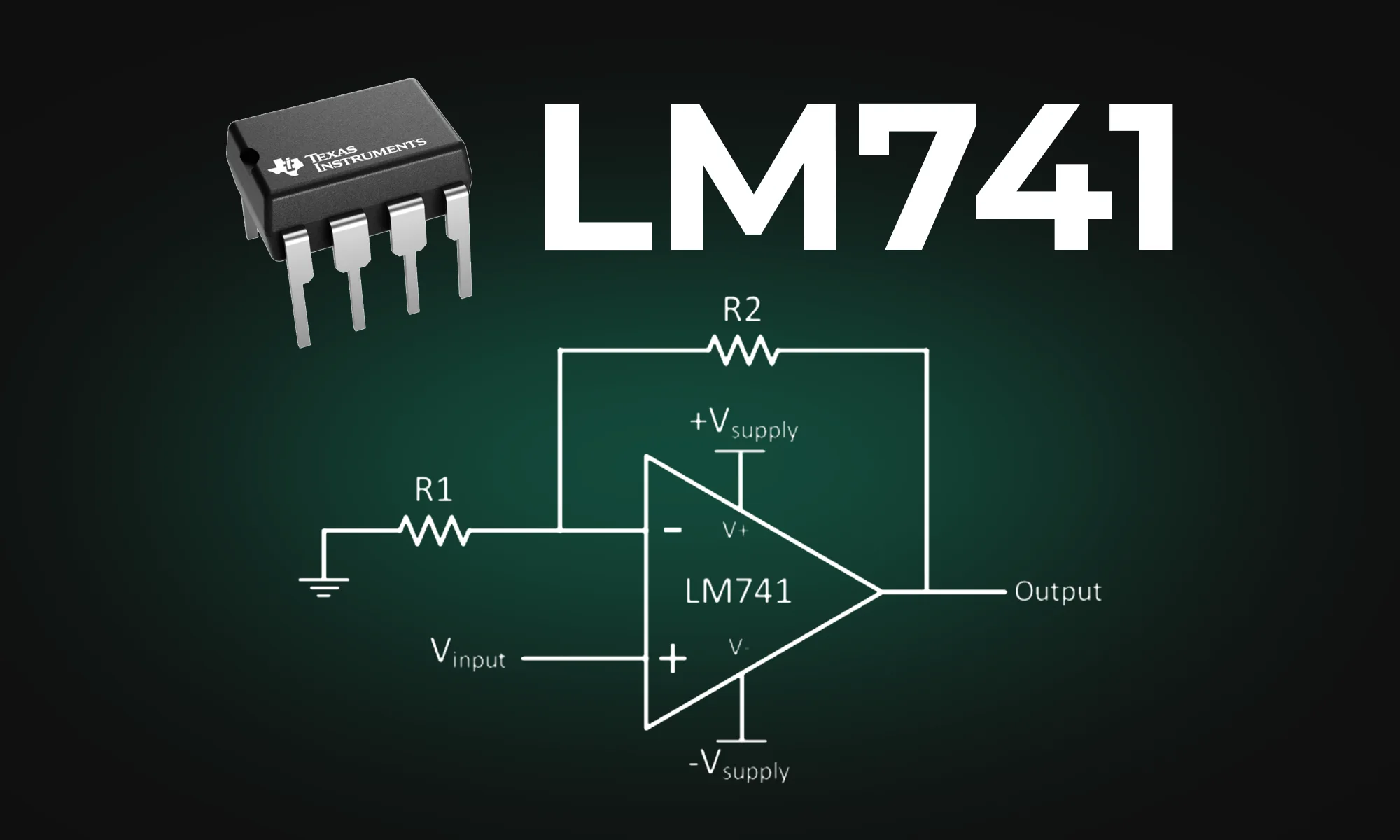
The blog post provides an in-depth look at the LM741 pinout diagram, explaining the functions of each pin, including inverting and non-inverting inputs, and comparing the LM741 to the LM324. It also covers various applications of the LM741 as an amplifier and a comparator.
Before we dive into the pinout, let's clarify what an op amp is. An operational amplifier is a type of amplifier that takes a voltage input and provides an amplified voltage output. The degree of amplification is determined by the circuit configuration and the external components connected to the op amp. Now that we've set the stage, let's explore the pinout diagram of the LM741.
Understanding the pinout of an integrated circuit like the LM741 is crucial for proper application. A pinout diagram visually represents the functions of each terminal or pin on the IC. The LM741 typically comes in a Dual In-Line Package (DIP), but it is also available in SOIC (Small Outline Integrated Circuit) form. Whether you're looking at a DIP or SOIC package, the pinout remains nominally the same.

One of the first things to note on the LM741 pinout diagram are the inverting and non-inverting inputs. The inverting input is where the signal to be amplified is often fed when you're building an inverting amplifier circuit. Conversely, if you're designing a non-inverting amplifier, you'll use the non-inverting input.
The LM741 pinout also includes terminals for connecting the positive and negative voltage supplies (V+ and V-), essential for the amplifier's operation. Always consult the datasheet, often found on a .org or .com website, for the recommended voltage levels.
The offset null pins are used for offset voltage adjustment, critical in applications that require high precision. Offset is the dc voltage difference between the inverting and non-inverting inputs when the output is nominally zero volts.
The output pin provides the amplified voltage signal. Depending on the circuit configuration, the output can be in phase or out of phase with the input.
The LM324 is another popular opamp often considered alongside the LM741. While both are operational amplifiers, the LM324 has four opamps in a single IC, compared to the single opamp in an LM741. This allows for more flexibility in circuit design but complicates the pinout slightly.
You can use the LM741 in a variety of circuit applications, not just as an amplifier. For instance, it can function as a voltage comparator. A comparator takes two voltage inputs and outputs a voltage indicating which input is higher. In this role, the LM741 offers less precision than dedicated comparators but is often sufficient for simple tasks.
So there you have it, a comprehensive look at the LM741 pinout and its many applications, from its use as an amplifier to a comparator. This IC is not just a basic operational amplifier but a versatile component suitable for a wide range of voltage amplification and comparison tasks. Whether you’re a seasoned engineer or just starting out, the LM741 remains an essential tool in your electronics toolkit.
Remember, before plugging anything in, always refer to the pinout diagram and other resources from trusted .org or .com websites to ensure you're connecting everything correctly. Happy building!
The LM2596 is a versatile voltage regulator used in various buck converters and power supply applications. The blog explores its key components, such as inductors, capacitors, and FETs, and provides insights into its broad voltage capabilities.
The LM2596 is essentially a voltage regulator designed as a buck converter. It can handle input voltages up to 40V, efficiently stepping them down to produce a lower, stable output voltage (Vout) that can be as low as 3V or as high as 35V. Thanks to its FET technology, the converter can achieve excellent regulation performance.
The LM2596 is an integrated circuit (IC) designed to function as a voltage regulator in a buck converter topology. While you won't be able to see the internal components just by looking at the chip, its datasheet will reveal a variety of built-in features that facilitate voltage conversion and regulation. Here's a general breakdown of what's inside:

The LM2596 typically incorporates an internal power N-channel Field-Effect Transistor (FET) that acts as the switching element. This FET allows the LM2596 to switch current paths, thereby stepping down the voltage.
The internal control logic manages the timing and switching operations. It usually operates at a fixed frequency and is responsible for the opening and closing of the internal FET.
The LM2596 includes a feedback loop that measures the output voltage (Vout) and compares it to a reference voltage. Any deviation results in an error signal, which is amplified and used to adjust the duty cycle of the switching FET to keep the output voltage stable.
An internal voltage reference sets the standard against which the output voltage is compared. This is essential for the regulation process.
Some versions of the LM2596 include built-in features for thermal shutdown and current limiting to protect the IC and connected components from damage.
Although the LM2596 itself is an integrated package, its effectiveness in a buck converter circuit relies on external components like inductors, capacitors, and sometimes diodes and resistors. The IC has pins to connect these components.
The LM2596 can handle a wide range of input voltages. Whether it's a 50V input from a power converter or as low as 5V, the LM2596 ensures a reliable output.
Vin is the input voltage fed into the circuit, while Vout is the output voltage regulated by the LM2596. This makes it extremely versatile, catering to both high and low voltage requirements.
Power supply units often incorporate this DC-DC converter for its synchronous regulation capabilities. The LM2596 is capable of driving up to 5A in specific conditions, which is quite sufficient for many types of electrical loads.
Different voltage ratings like 25V, 30V, and 35V for electrolytic capacitors are often employed based on the desired output and input voltage ranges.
Voltage ripple is an essential factor to consider, and the LM2596 excels in maintaining a low ripple, thereby ensuring a stable output.

Different inductor types or core materials produce different amounts of this characteristic ringing or ripple. Ferrite coreinductors have very little core loss and therefore produce the most ringing. The higher core loss of powdered ironinductors produce less ringing. If desired, a series RC can be placed in parallel with the inductor to dampen theringing.
The LM2596 operates at a fixed frequency, aiding in easier filter design. The chip incorporates internal switching transistors, further simplifying the circuit topology.
Datasheets and Webench tools are useful resources for understanding the LM2596 circuit's pinout and diagram. Datasheets provide detailed specifications, while Webench helps in simulation and layout design for your PCB.
MOSFETs can be used in more advanced configurations to handle even higher power applications.
The synchronous buck converter version of LM2596 employs two FETs for enhanced efficiency, compared to standard buck converter topology.

The LM2596 is a versatile and robust DC-DC converter, central to many power supply systems and voltage regulator applications. Its excellent performance, including a broad voltage range of up to 50V and low ripple, make it a preferred choice. Whether you're focusing on inductor specifications, capacitor types, diode characteristics, or FET functionalities, this IC has proven itself as an efficient voltage regulator in both asynchronous and synchronous settings.
Before diving into your project, make sure to refer to datasheets for the most accurate information. Diagrams are your best friend when laying out your PCB. Remember, you can use the LM2596 in adjustable setups by modifying the resistor values to achieve custom voltage outputs.
LM2596 offers a reliable and efficient solution for all your voltage regulation needs, serving as the cornerstone in many buck converter and power converter applications.
Explore the mechanics of converting AC to DC in this comprehensive blog post. The article covers everything from the role of transformers in adjusting voltage levels to the function of bridge rectifiers and capacitors in shaping the waveform.
Alternating current is a form of electrical energy where the electric current and voltage oscillate in a sinusoidal or sometimes non-sinusoidal waveform. This is different from DC, where the electrical energy flows in one direction.
George Westinghouse was an early adopter and proponent of alternating current. He championed the concept of using AC electricity over DC because AC voltages can be transformed easily, making it more adaptable for long-distance transmission.
The process of converting AC to DC often begins with a transformer. Transformers are critical in modifying the voltage levels. For instance, a 12V AC supply can be stepped down to a 5V AC supply using a transformer.

Once the transformer adjusts the AC voltage, a rectifier takes over to convert this AC into DC. The most commonly used type of rectifier is the bridge rectifier. This device uses four or more diodes arranged in a specific manner to ensure that the electrical energy flows in one direction, converting the alternating current into a form of direct current.

The sinusoidal waveform of alternating current when passed through a bridge rectifier tends to get converted into a square wave. This square wave still contains AC components that are not suitable for DC electronic devices.
Interestingly, a power inverter can do the reverse of a rectifier. It takes DC and changes it back to AC. You might wonder why convert it back to AC? Well, some applications require the DC to be converted back to alternating current, such as in the case of a DC to AC power inverter.

The square wave output from the bridge rectifier is still not a pure DC. This is where a capacitor comes into play. By using a capacitor in the circuit, the square wave can be smoothed out into a voltage level that more closely resembles a DC signal.
In power electronics, `displaystyle` is often used to represent complex waveforms mathematically. This is crucial for engineers who are designing or understanding a circuit for an AC to DC converter. Understanding the waveform, whether it's a sine wave, square wave, or any other form, is crucial for the efficient conversion of electrical energy.
When dealing with AC and DC, the units like hertz (Hz) and volt (V) become very important. For instance, in the United States, the standard power supply frequency is 60 Hz with a voltage of around 110-120V. A power converter will take this and convert it to a 12V or 5V DC power supply, depending on the requirement.
In advanced circuits, after the action of a rectifier and capacitor, a voltage regulator may be used to ensure that the output DC voltage remains constant regardless of fluctuations in the input AC voltage. This is particularly useful for sensitive electronic devices that require a stable power supply.

Many of the chargers for our electronic devices like laptops and smartphones are essentially AC DC converters, acting as an adapter between the AC supply and the DC power supply needed by the electronic device. Some specialized converters even offer the function of a DC to DC converter, which can adjust DC voltage levels just like a transformer does for AC.
Before the widespread use of semiconductors, a commutator was often used to convert AC to DC. The commutator reverses the direction of electric current twice during each cycle, mimicking a sort of mechanical rectifier. However, in modern power electronics, solid-state devices like diodes have largely replaced commutators.
The AC to DC converter plays a vital role in our lives, ensuring our electronic devices get the right kind of power. From the use of transformers and bridge rectifiers to the role of capacitors and voltage regulators, the intricacies are many. As we continue to rely on an increasing array of electronic components, the need for efficient and reliable converters will only grow. Understanding how they function is not just for electrical engineers but anyone who wants to grasp how our modern world is powered.
The blog is an educational resource on netlists, detailing their role as intermediaries between circuit schematics and physical layouts. Special attention is given to different types of netlists, such as FPGA and RTL. It outlines the crucial role of accurate netlists in hardware functionality and discusses the various formats used in the design process.
A netlist is essentially a textual representation of an electronic circuit. It describes the connectivity between different components, such as transistors, resistors, and capacitors, without necessarily detailing their physical arrangement. Think of it as the "source code" for a circuit, providing the essential information needed to understand how the circuit functions.
In circuit design, netlists serve as the intermediary between the schematic and the physical layout. Once a schematic is complete, it gets converted into a netlist, which can then be used for simulation, analysis, and eventually, physical layout generation.
To further understand the concept, consider a netlist as akin to a recipe in cooking. The recipe lists the ingredients (components) and explains how to combine them (connectivity), but it doesn't tell you how to physically arrange them on the plate.
In circuit design, a netlist acts as the blueprint for hardware implementation. It specifies how components are interconnected, thereby defining the circuit's functionality.
Netlists are crucial for various stages of hardware development, including simulation for performance analysis, logical synthesis for gate-level representation, and physical synthesis for layout generation.
An inaccurate or inefficient netlist can lead to hardware that doesn't function as intended, costing both time and resources. Therefore, generating and verifying an accurate netlist is a critical step in the design process.
Netlists can come in various formats, such as SPICE for circuit simulation and EDIF for interchange between different EDA tools.
A schematic netlist is derived directly from a circuit schematic and is more human-readable. In contrast, a structural netlist is a lower-level representation that describes the circuit in terms of gates and flip-flops.
Choosing the right format is crucial as it impacts the tools you can use for simulation and synthesis, thereby affecting the overall efficiency and accuracy of the design process.
An FPGA netlist describes the configuration and interconnection of logic blocks within an FPGA (Field-Programmable Gate Array). It is specifically tailored for the architecture of the FPGA in use.
An RTL netlist describes the circuit at the register-transfer level, focusing on how data moves between registers and how the logical operations on the data occur.This could be defined in hardware definitions (HDLs) like Verilog or VHDL.
FPGA netlists are essential for FPGA design and simulation, while RTL netlists are crucial for high-level synthesis and system-level descriptions.
An RTL netlist provides a high-level abstraction of the circuit, making it easier to understand and optimize the design for specific objectives like speed or power consumption.
Unlike schematic or structural netlists, RTL netlists allow for a more abstract representation of the circuit, focusing on data flow rather than specific gates or components.
RTL netlists are invaluable for system-level simulations and verifications, as they allow designers to test how individual components interact within the larger system.
In conclusion, netlists serve as the linchpin in the complex world of electronic circuit design, functioning as the textual blueprint that outlines the vital connections among various passive and active components like transistors, resistors, capacitors, and integrated circuits. They bridge the gap between the conceptual world of schematics and the concrete physical layouts, playing an important role at multiple stages, from simulation and logical synthesis to the generation of the final hardware layout. Their formats may vary, with options like SPICE for circuit simulation and EDIF for tool interchange, each bringing their own set of capabilities and limitations.
Specialized netlists, such as FPGA and RTL netlists, address specific design needs and provide varying levels of abstraction to better suit project objectives. An accurate and efficiently-structured netlist is not just a nice-to-have but a necessity, as errors can lead to functional issues in the hardware, costing time and resources. Understanding the intricacies of netlists, therefore, is not merely an academic exercise but a practical necessity for anyone involved in PCB design.
Oscillators are electronic circuits producing oscillating signals without an input. Types include sine, square, sawtooth, triangular, and pulse wave oscillators. Crystal oscillators use vibrating crystals for precise frequencies, crucial in clocks and radios. RF oscillators operate at radio frequencies, essential in broadcasting and telecoms.
Oscillators can be categorized based on the type of output waveform they produce:
Crystal oscillators are a type of oscillator that uses the mechanical resonance of a vibrating crystal to create an electrical signal with a precise frequency. This frequency is commonly used to keep track of time, as in quartz wristwatches, to provide a stable clock signal for digital integrated circuits, and to stabilize frequencies for radio transmitters and receivers.
The oscillator circuit is the heart of the oscillator, containing all the components necessary for the generation of the oscillation. The feedback mechanism is a crucial part of this circuit, as it is responsible for maintaining the loop of signal that results in oscillation.
The oscillation frequency is determined by the components of the circuit (such as inductors, resistors, capacitors, BJT, and FETs), and the selection of these components is crucial to the operation of the oscillator. For a Colpitts oscillator circuit, for example, the design can aim to exploit the natural resonance of a resistor, inductor, and capacitor (RLC) network to create oscillations. The tuning procedure involves adjusting the components to achieve the desired frequency.
RF oscillators, or Radio Frequency oscillators, generate an AC signal at radio frequency. They are used in a variety of applications, including radio and television broadcasting, cell phones, and satellite communications.
There are several types of RF oscillators, each with its own set of design considerations. The application of the oscillator in the radio frequency circuit design will determine the type of RF oscillator used.
Oscillators are a cornerstone of modern electronics, playing a crucial role in a wide range of applications. As technology continues to advance, so too will the capabilities and applications of oscillators. Understanding the basics of oscillators and their operation is a stepping stone to understanding more complex electronic systems and circuits. The future of oscillator technology promises exciting developments and further integration into our daily lives.
Discover how Flux.ai enhanced its web app performance using the open-source tool, log-time-to-next-idle. The blog details how to measure user interactions and pinpoint their completion point for optimal performance. Learn from our experience and apply these strategies to refine your app's user experience.
Flux.ai is a complex, single-page web app that helps electronic engineers design printed circuit boards. As with any professional design tool, it needs to be fast, precise and predictable.
Early versions of Flux.ai were noticeably slow. We set a goal of making all our user interactions take less than 100ms, supported by science. We started a plethora of projects to make that happen, one of which I wrote about in another blog post. To make sure these efforts paid off, we created a measurement tool, log-time-to-next-idle, that is the subject of this blog post.
We've been using it to track the performance of around 50 key user interactions over 18 months, such as:
We're very happy with how it is working. And now we've shared it with the world as an open-source package.
A user interaction is defined here as any input the user provides—mouse click, key press, and so on—coupled with the intended effects of the input—menu opened, element added, and so on. The performance of a user interaction is simply the time between the start of the input to the end of the effects. For example, clicking on a select box will open a menu. The interaction is done when the menu has finished loading.
A subset of the interaction time is defined as “frozen time”. This is the interval following the user input when there are zero screen updates––no animation frames.
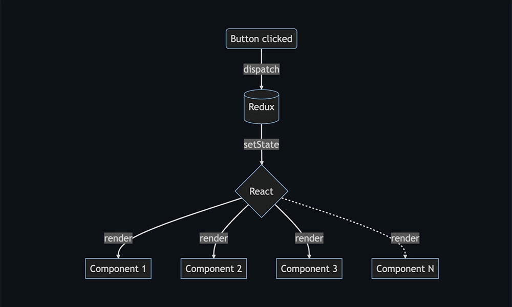
Although the concept of a user interaction is easy to define intuitively, the end state can be hard to define formally. In modern reactive UIs, any part of the UI can freely change in response to an update of a store of application state (Redux, Zustand, and so forth). The initial handler of some user input doesn't know all the downstream effects of its execution and so it can't mark the end of the interaction.

In the diagram above, it is hard to know which among the N components will determine the "end" of the interaction. You may not even know what are all the N components that react to some user inptu. To deal with this problem, we took a shortcut. Assuming that...
...we can leverage requestIdleCallback to mark when an interaction is done.
Similarly, we can leverage requestAnimationFrame to indicate when an interaction has yielded control back to the main thread, unfreezing the UI.
In short, log-time-to-next-idle measures user interactions by queuing a requestAnimationFrame and a requestIdleCallback at the start of an interaction, then recording the time when the callbacks fire.
Just put a call to logTimeToNextIdle at the start of any event handler. Here is an example of logging the time it takes to switch fictional tabs in a React app.
log-time-to-next-idle deals with overlapping interactions by cancelling earlier queued callbacks. In other words, the last interaction "wins" and any previous in-progress interaction is ignored. For ease of interpretation, you should try to measure debounced interactions that happen one at a time.
log-time-to-next-idle will store measured intervals in the browser using window.performance.measure (if available). The intervals will then show up in the profiler (if available).
Here is an example that logs to the console when in dev build mode, and logs to somewhere in the cloud when in prod build.
We hope this measurment function log-time-to-next-idle will be useful to you and your app, as well as the general approach of defining interaction end points in terms of CPU usage. Check out the open-source package and please post any feedback there.