May 8, 2025
Smart Polygons: Advanced PCB Design Just Got Easier
Share
BuildWithFlux


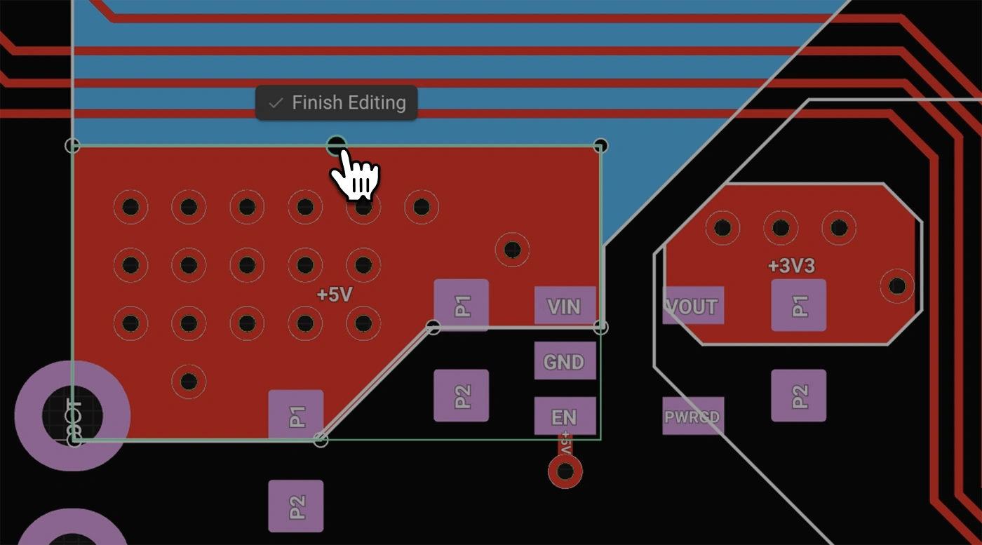
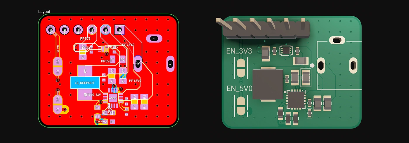
Smart Polygons in Flux behave intuitively like traces, making them straightforward to learn and use—start directly from any pad with automatic net association, simply click to place and adjust points, and watch as copper intelligently reflows in real-time. Let’s dive in!
In PCB design, polygons are customizable copper shapes directly tied to a specific net. They’re crucial because they significantly influence the electrical performance and reliability of your PCB. Polygons allow you to optimize your board layout for specific electrical properties, including improved grounding, controlled impedance, and efficient heat distribution.
Specifically, polygons are indispensable for:
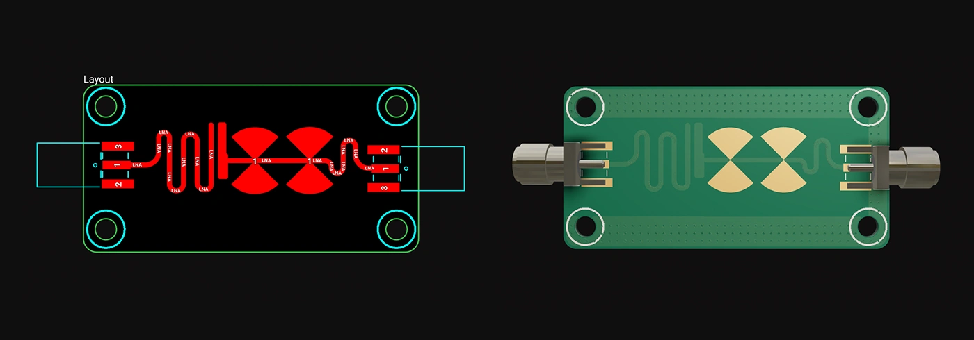
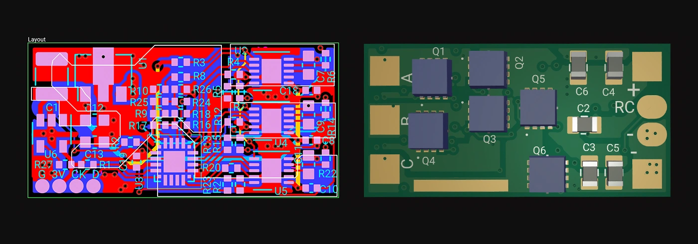
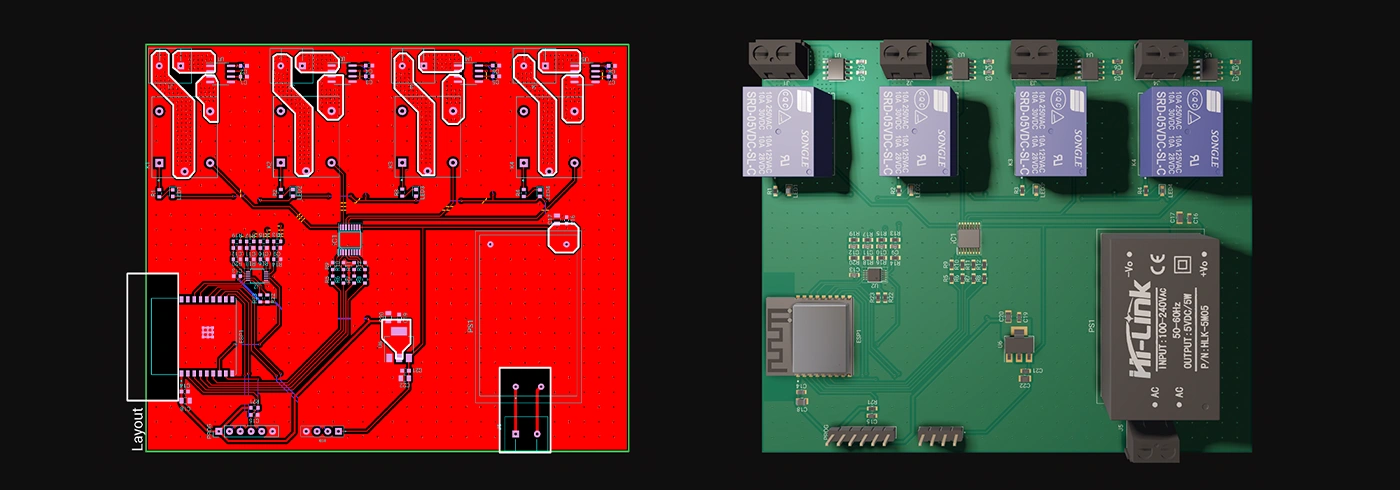
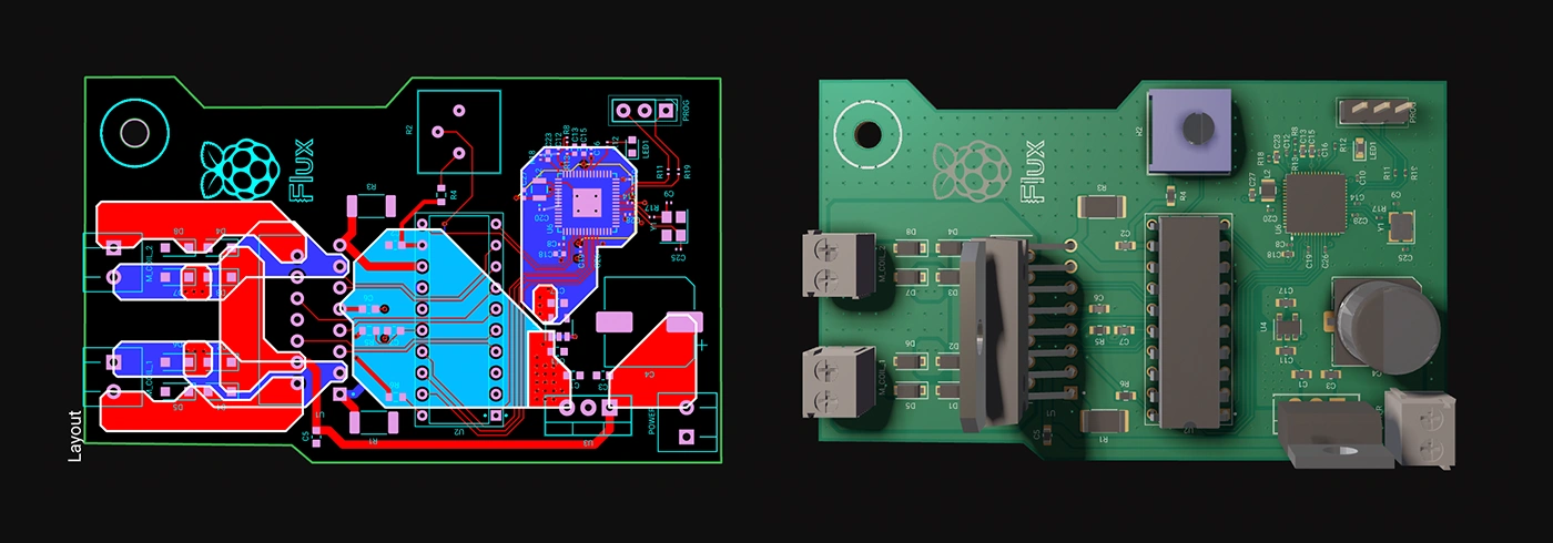
{{polygons-examples}}
Unlike zones—which define areas where copper cannot exist—polygons actively conduct electricity and shape your board's electrical performance, making them fundamental for advanced PCB designs.
At Flux, we prioritize intuitive, user-friendly workflows. Automatic copper fills were the first step. Now with polygons, we've continued this approach:
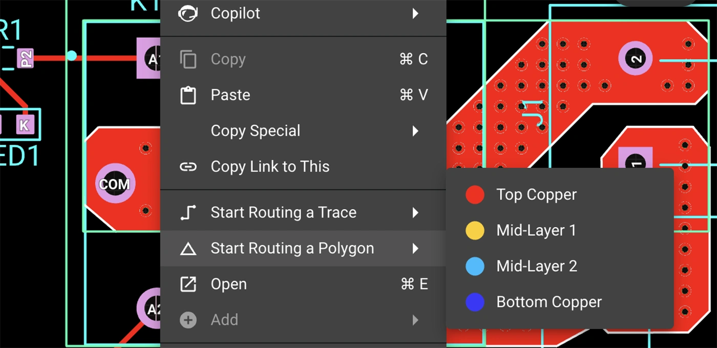
Polygons in Flux behave intuitively like traces, making them straightforward to learn and use, right from the start.
Polygons in Flux pack powerful functionality without complexity:
Polygons unlock new possibilities in your PCB designs. Here are a few practical ways you'll benefit:
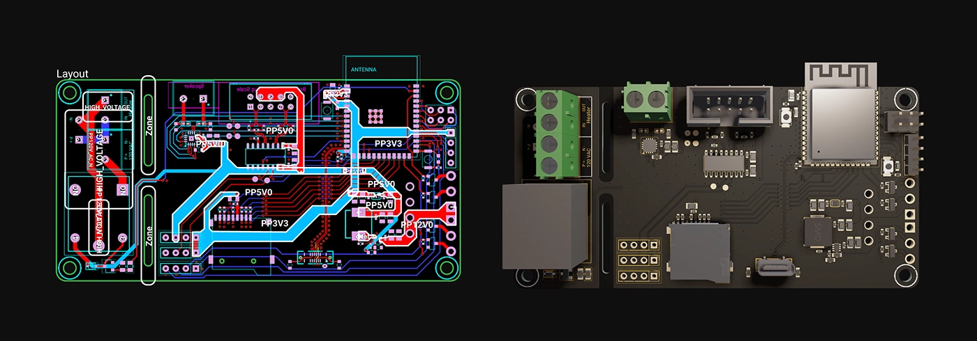
Whether you're just dipping your toes into PCB design or you’re a veteran engineer tackling complex layouts, polygons in Flux offer the ideal balance of simplicity and capability:
Polygons are available now in Flux, ready to enhance your PCB design capabilities. Explore this powerful feature today and experience firsthand how advanced design can truly be this easy.
Dive in now and check out our detailed polygon documentation or jump straight into Flux to try it yourself. We can't wait to hear what you think!


Today, we're thrilled to unveil Copilot Experts – a new suite of specialized AI models, each fine-tuned for specific tasks to deliver sharper accuracy and faster performance. Now, you have the power to easily select the AI model that best suits your current task, ensuring more precise and swift responses.

Design review is one of the most time-consuming and expensive parts of the hardware design process. Most engineers spend over 30% of their time performing design reviews. What if we could reduce that so that products could ship 30% faster and 30% cheaper?

Today, we’re thrilled to launch a powerful new feature that allows you to declare project requirements like operating temperature, voltage, or compliance standards so Copilot can leverage that knowledge to accelerate tedious tasks like BOM verification, debugging, and part recommendations freeing you to do more of the work you love.
We’re incredibly excited to announce that we have decided to open up Flux and move out of private beta! What does this mean? If you’re a current user of Flux - nothing will change for you. For new users, this means that we’re now allowing anyone and their team to signup!

Today, we’re announcing Flux Enterprise, a new plan that allows enterprise hardware teams to leverage AI to iterate faster, streamline processes, mitigate risks, and enhance team efficiency. With Flux Enterprise, we’re finally bringing AI to hardware teams at enterprise companies with Flux Copilot.
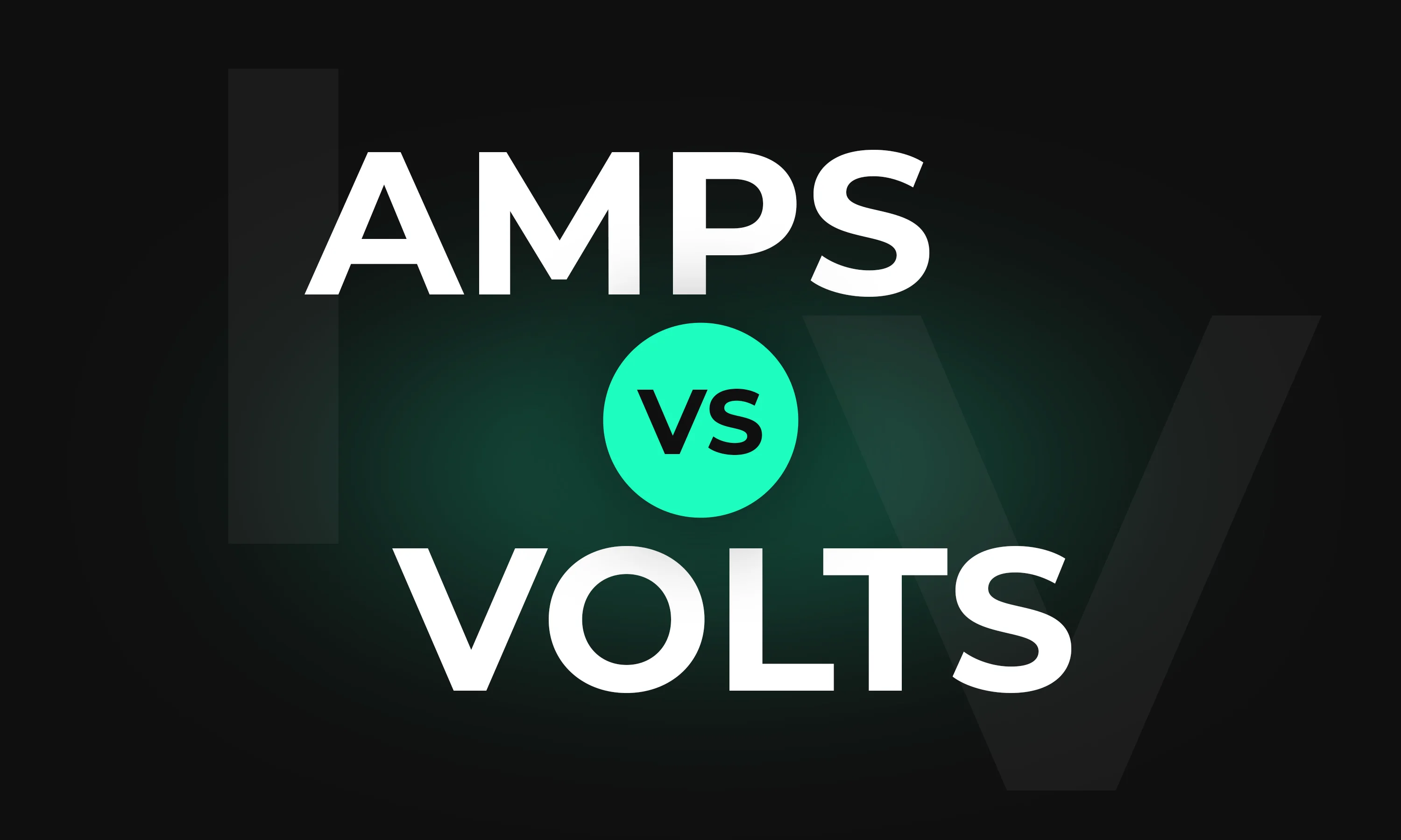
Understanding amps and volts is key to working with electronics. This guide explains their roles, relationship, and practical applications.

Buck and Boost converters are highlighted for their power efficiency and system reliability roles. The blog reveals their unique advantages, making them essential in diverse applications like renewable energy and portable electronics.

The blog is an educational resource on netlists, detailing their role as intermediaries between circuit schematics and physical layouts. Special attention is given to different types of netlists, such as FPGA and RTL. It outlines the crucial role of accurate netlists in hardware functionality and discusses the various formats used in the design process.